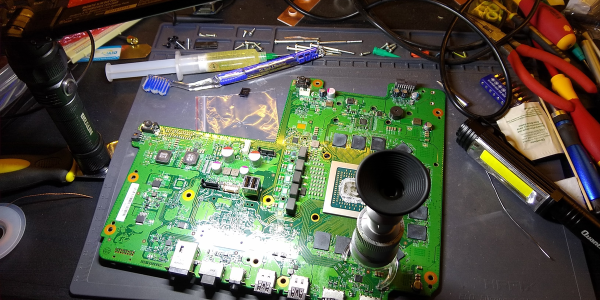
There can be few among those of us who produce printed circuit boards, who have not at some point placed a component the wrong way round, or with the wrong footprint. Usually this can be rectified with a bit of rework and a fresh board spin, but just occasionally these mishaps make it into the wild undetected. It seems nobody is immune, as [Doug Brown] is here to tell us with a tale of an Apple product with a misplaced capacitor.
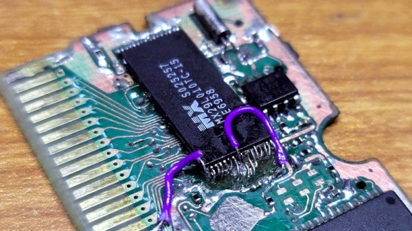
The LC series of Macs came out through the early 1990s, and their pizza-box style cases could be found slowly turning yellow in universities and schools throughout that decade. Of them there was a persistent rumor of the LCIII had a misplaced capacitor, so when he received an unmodified original machine he took a look. The investigation is quite simple, but revealing — there are three power supply rails and one of the capacitors does have a significant leak.
The explanation is simple enough, the designer had placed a capacitor on each rail, with its negative side to the ground plane, but one of the rails delivers -5 volts. Thus the capacitor is the wrong way round, and must have failed pretty early in the lifetime of each LCIII. We’re curious then since so many of them went through their lives without the component being replaced, how the circuit remained functional. We’re guessing that there were enough other capacitors in the -5 volt line to provide enough smoothing.