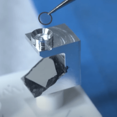
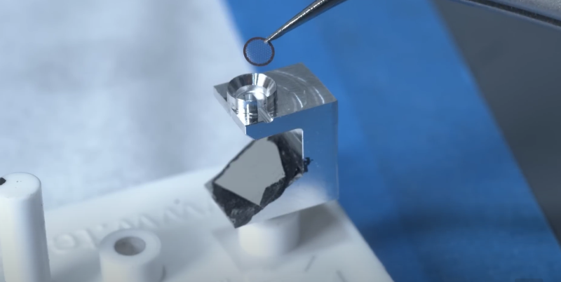
Some of you probably know this already, but there’s actually more than one kind of electron microscope. In electronics work, the scanning electron microscope (SEM) is the most common. You hit something with electrons and watch for secondary electron emissions. However, biologists more often use a TEM — a transmissive electron microscope — which passes electrons through a sample to image it. [Breaking Taps] built a small device to convert his SEM into a TEM.
One key idea is that in a SEM, the beam’s position on the target is the only thing that matters. Any secondary electron detected is a result of that spot’s composition, no matter where you collect them. Common detectors pick up back-scattered electrons bouncing back toward the electron source. There are also low-energy electrons bouncing off in random directions, depending on the topology of the target.
 The slow electrons can be attracted by a single detector that has a strong positive charge. TEM doesn’t detect secondary electron emissions. Instead, it passes electrons through a target and collects the ones that pass through a very thin sample using a screen that glows when electrons hit it.
The idea, then, is to create a STEM-SEM device. There’s a sample holder and an angled reflector that shoots electrons passing toward the SEM’s detector. The back-scatter detector is not used, and a shield prevents the detector from seeing secondary emissions from the target itself.
You can buy these, but they are well over $1,000, so in true hacker fashion, [Breaking Taps] made his own. You could, too, but you’d need a pretty good machine shop and — oh yeah — a scanning electron microscope.
While we have seen some home labs with electron microscopes, you need some high-tech vacuum and high-voltage gear, so it isn’t too common. Armed with a STEM, you can even see the shadows of atoms.


A highly related topic that I’d love to see on hackaday is making your own direct electron diode detector (and necessary electronics).
FWIW, here is a link to the paper on conversion detectors by Reimer:https://doi.org/10.1002/sca.4950020406
Uhh, that was not the paper I thought it was. Here is the one I meant:
https://doi.org/10.1002/jemt.1060050105
By Oho.
We have one of these. One disadvantage is that a regular SEM has a maximum accelerating voltage of ~30 kV, and a TEM usually runs into hundreds of kV. Don’t get me wrong, this capability is handy on an SEM, however it can’t really replace a TEM.
Right. That was my first thought as well. That being said low energy is great for bio. But then you have to cool it.
I have been using an ancient Philips xl30 environmental sem for bio samples. No freezing, no gold sputtering. Just samples in and wait a bit longer to get the moderate low vacuum. Using the back scatter detector or normal.
I’m working on it too. You just put the resin sample simply cut with the ultra microtome. No TEM or carbon staining on the surface?
You guys, being savvy on EMs may be able to point me in the right direction; I’m more than ignorant and pre-apologize for posting to an experimental application group. The pickens are slim on EMs.
Why would anyone bid on, what was listed as an Electron Microscope, something they know zilch about? Because you can, I did, and I won.
The unit is palated, stands about 1 meter high, has a label saying Raymond Control Systems Inc. (RCS). It has an additional larger name sticker “M2” with bars over both characters.
I’ve read enough, I’m an EE, when it arrives I will determine if it’s TEM or SEM; this I’ve read up on and can do.
Where can an EM neophyte turn to?
Pre-Thanks for any direction