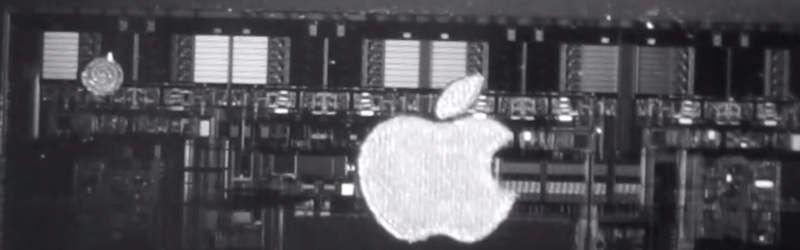
If you want to see inside an integrated circuit (IC), you generally have to take the die out of the package, which can be technically challenging and often destroys the device. Looking to improve the situation, [Bunnie] has been working on Infra-Red, In Situ (IRIS) inspection of silicon devices. The technique relies on the fact that newer packages expose the backside of the silicon die and that silicon is invisible to IR light. The IR reflects off the bottom metalization layer and you can get a pretty good idea of what’s going on inside the chip, under the right circumstances.
As you might expect, the resolution isn’t what you’d get from, say, a scanning electron microscope or other techniques. However, using IR is reasonably cheap and doesn’t require removal from the PCB. That means you can image exactly the part that is in the device, without removing it. Of course, you need an IR-sensitive camera, which is about any camera these days if you remove the IR filter from it. You also need an IR source which isn’t very hard to do these days, either.
Do you need the capability to peer inside your ICs? You might not. But if you do and you can live with the limitations of this method, it would be a very inexpensive way to get a glimpse behind the curtain.
If you want to try the old-fashioned way, we can help. Just don’t expect to be as good as [Ken] at doing it right away.


This would be great for detecting fake chips. Package it together to make it portable, and bring it on your shopping trips at the SEG.
Unfortunately this only works for flip-chips without encapsulation or lidding. This won’t help you weed out clone STM32s unless you’re interested in CSP footprint parts.
– Concept is fascinating
– thanks both to [Bunnie] for making it work, and [Al Williams] for sharing it
– is this the sort of thing that might be useful to governments to use alongside destructive testing, to make sure no one slips sneaky backdoors into their supply-chain?
– I only ask because I’d like to make sure [Bunnie] was exposed to all available grant funding they might need!
– I realise that constraints of the technology, imposed by physics, may be insurmountable, and limit use to classes of chip that tend not to do Big Secret Things in Big Secret Projects, so it may be of little relevance; I’m just a chip ignoramous so I’ve no idea about such things.
It’s kind of neat this works with ‘normal’ silicon cameras. It’s operating in a tiny slice of spectrum around 1050nm, where the silicon in the object is transparent enough to see through, but the silicon in the camera can still absorb enough to detect the photons.
If it were the silicon you were interested in seeing then you’d need a different wavelength of light, fortunately the silicon is pretty uninteresting and the bits we do want to see aren’t silicon.
Ditto with an image sensor, the silicon isn’t doing the heavy lifting, it’s the structures foremd, deposited, etched into it that are doing the heavy lifting of light sensing
Sez CJay: an image sensor, the silicon isn’t doing the heavy lifting
Uh, no. The silicon in an image sensor is ABSOLUTELY doing the ‘heavy lifting’. That’s where the photons get absorbed and the requisite electrons get liberated to get detected. The structures created in the silicon just store the electron charge to be read out, and then do the charge-to-voltage conversion that is the image signal.
Make no mistake, it’s the silicon doing the detecting. Which is why a silicon-based camera is blind at wavelengths longer than 1100 nm.
Very impressive hack.
I wonder if stacking or super resolution technic of some sort could use multiple images of low resolution to enfance the resolution ?
Not likely.. the low quality you see is probably due to poor optical performance of the imaging system at the wavelength of 1 micron. Remember that most consumer imaging systems are designed for the visible spectrum (if you’re on a budget at least). If you change the illumination to be outside this range then the optical performance will suffer. Imaging at 1 micron is possible, but to achieve better performance requires a re-design of the optics (different elements, spacing, and materials).
Many “regular” lenses don’t work that well at 1000 nm, but some do work well. The Raspberry Pi HQ 6mm C (or CS?) lens is sharp in the center, the new RPi Camera Module 3 NoIR lens is very good, and I’ve also had good luck with some Rokinon/Samyang mirror less camera lenses.
https://github.com/williamhobbs/PVRW-2023-EL
And isn’t there a fundamental resolution limit of about 1um if using 1um light?
This immediately reminded me of a very old sci-fi movie: “The Man With X Ray Eyes”.
Fantastic film, Ray Milland was brilliant in it.
If your fake IC deceives you, pluck it out!
Is it safe to assume that this IR is a wavelength that can’t affect the gates of the transistors? The potential to affect the operation of an encapsulated device with a strong enough light source sounds like a problem (sort of like that RasPi 2 U16 chip issue from ages ago).
I tried to replicate this using a cheap usb microscope. I started by desoldering two ir leds from old remotes. Then removed the ir filter from the usb microscope. (It is a little plate that sits behind the pinhole of the Camera.) At first i had no luck. I asume the leds i used are around 960nm, so i ordered the 1070nm leds and i was able to see through the enclosure of the backside of a sd card, wich revealed the traces of the pcb inside. (Wich i think proofs it is basically working.) How ever i wasn’t able to see through ic enclosures. I tried various ics from boards i have laying around. some stm32 FXXX, Arduino Nano, A scrap Sat receiver, Latice FPGA, FTDI323, Nexus 5X Mainboard, …) But i couldn’t get any thing to reveal some parts of the die.
Has some one some ideas why this isn’t working?
I suspect that the dynamic range of this cheap camera isn’t as good as the camera used by Bunny.
Hi maxbit89, I had the same problem. I did not try the SD cards yet (I’ll do that this evening), but I ordered 3 of the LEDs used by Bunny (https://www.digikey.com/en/products/detail/marktech-optoelectronics/MTE7110N5/11205108), and used my modified Cannon Rebel with the IR filter removed (I use it for astrophotography), placed over the eyepiece of my AmScope binocular inspection scope using a tripod. I was not able to see through IC packages (tried op amps, RP4 processor, and some transistors). I was using 30sec exposures at 6400iso. I am not able to run longer exposures, but I am running a stacked image set now (300 images at 30sec each), I’ll see if I can get anything.
From what I can see, the images that I am getting are blown out by the amount of reflected light from the surface. Perhaps my imaging setup does not have enough dynamic range to capture the image.
I’ll let you know if I figure something out.
Did you note the part that says ” The technique relies on the fact that newer packages expose the backside of the silicon die and that silicon is invisible to IR light. ” ?
This isn’t magic eyes capable of seeing through a plastic-encapsulated package.
I did not realize that. I thought the DIP package epoxy was transparent to IR. Thanks for the clarification!
Could that range of light passing silicon be used as an attack vector on silicon photonic chips, light being the interfiering force? Could bits be flipped by fuzzing, following quantum mechanics?