One of the most laborious tasks in PCB layout is the routing. Autorouting isn’t always perfect, but it is nice to have the option, even if you only use it to get started and then hand-tune the resulting board. Unfortunately, recent versions of Kicad have dropped support for autorouting. You can, however, still use Freerouting and the video from [Mr. T] below shows you how to get started.
There are three ways to get the autorouting support. You can install Java and a plugin, you can isntall using a ZIP file, or you can simply export a Specctra DSN file and use Freerouting as a standalone program. Then you import the output DSN file, and you are done.
Not only does [Mr. T] show you how to do a simple USB board, he also shows you how to rip up the autorouter’s work if you don’t like it. He also covers some tips to get the best results with the router.
For example, it is often advantageous to manually layout a few critical tracks before you run the autorouter. You can also use net classes to specify parameters for some tracks.
Overall, this is a worthwhile thing to do. After all, you don’t have to use autorouting, but it is nice to have it available if you want it. If you don’t like Freerouting, you can try a different solution. Of course, these routers use DSN, so you can use them with many different tools if you aren’t using Kicad.


> One of the most laborious tasks in PCB layout is the routing
Actually, I find the most laborious task is copying shapes and components from the datasheets, especially when the measurements are unclear or missing.
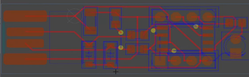
An essential part of good routing is component placement, and I think it’s much harder to do good component placement if you’re not doing the routing yourself. In the example, C1 should be moved closer to the chip (it’s a decoupling cap, should be next to VCC pin). Then D1 should be moved to where C1 is, and D2 to where D1 is. Once you get all the components placed well, the actual routing for this example becomes straightforward. When placing the components, I recommend looking at the schematic so you understand the function of each component, and can place it so that it performs that function well, and the signals flow naturally over the board.
I found autorouting to be very useful when it comes to component placement. I give it a go, see where bottlenecks are, and iterate. Only after all other things are done, a final autoroute touched up by hand. Guess everyone has a workflow and all projects are different, but routing indeed only last step taking only a day or two after weeks of work.
In addition to the really good. Comment Artenz wrote, layout/routing can be therapeutic. Also who doesn’t love to see a beautifully routed board? Its craftmanshil and skill.
Just looking at the header image, who would routes that D+ signal from the pad like such?
Autorouters are a bit like AI. You end up spending just as much time holding their hand to get it right. But sometimes they can help/hint by giving some good ideas.
P.S. isntall? :p
I never met any seasoned electronic engineer really using an autorouter.
I think autorouting is just the first baby step towards complete pcb generation. We just need to be able to specify more constraints while doing the schematics, for example we should be able to specify fonctions of component like decoupling cap at schematic level so the autogeneration knows were to place them, also any constraints on special traces… And on pcb side, we should be able to place the few components that actually have placement constraints regarding mechanical (like connector, button, sensors, pcb size/shape,…) and let everything else free floating. If we can have a way to specify more precisely what an autogenerator should do it could definitely do. We have to stop thinking human are more clever than computer for such repetitive tasks, it’s the case right now only because we don’t provide all the info we have to the computer.
+10, exactly this and I think that it is the same for mechanical part with all the generative design (even though I’m not convinced the way it is done actually)
I agree with you to a certain extend, except for the last part. Human are more clever than computer ; computer are not clever, they are efficient.
And as long as humans are involved in the life cycle of a PCB (as user, controller, repairman, etc.), having a (competent) human designing it will ease the task of other humans coming after him.
Maybe a well designed software could do a better work at placing and routing components, but if explaining the machine what it is handling takes more time than doing it youself, where is the point ?
My friend is very skilled EE (both high voltage and embedded stuff, 20 years of work experience) and he is using autorouter only. He is puzzled like me why in the earth you want to do it manually.
How? There is no autorouter out there that can do high speed properly (impedance matched diff pairs, RF traces, etc.). And in any modern commercial board high speed is a very significant part of traces (for me often the majority of traces on a board).
How can someone with 20 years of experience only ever do hobbyist level low speed boards? I don’t believe you.
There’s a difference between a high speed pci bus for example that needs to go in a mass produced intel motherboard, and one that needs to just be good enough to work with a specific piece of hardware with only modest requirements. Plenty of people are only doing the latter, and besides, you could manually do that and autoroute the rest.
“Never trust the Auto-Router” :)
Latest KiCad has Autorouting plugin available via the PCM (Plugin Content Manager).
Not that I would ever use it.
My bad – I just saw the video. His first recommendation for FreeRouting is via PCM.
When autorouting becomes as easy at it is in Eagle, I can consider switching to kicad. I’ve never had any problems with Eagle autorouter. Yes by default it makes routes look a bit messy but as long as the board works I couldn’t care less what copper layers looks like.
If you have to deal with EMC/EMI (sometimes even between parts of your own design) the shape of the copper layers can determine if the board works or not.
As a punkster, I do route current carying tracks manually and autorouting all the rest, at least up to some tens of MHz. Am I therefore a Putin´s bitch?
Yes.
Huh? Did you ever have to do EMI certification? Your traces affect the EMI noise hugely. One too sharp corner for a 10MHz signal and you’re suddenly emitting 100MHz harmonics and fail your certification.
I have never used an auto-router for any kind of professional work but I do admit it is very therapeutic to watch it try to route a board through brute force
Let us see when (open-source) AI-routing is ready and can suggest better component placement with better routing. Until then, manual for the win
I was thinking about how you would go about making an AI based routing algorithm.
And my first though was Evolutionary Genetic Algorithms where you have many constraints (impedance matching, minimal or matched track lengths, minimal use of vias, clock rate) and breed the near optimal solutions over a very large number of generations for each trace on each board. The solutions would not look like any board that a human would ever design.
Or you just gain access to a very very very large number of human professionally designed PCB’s (ideally ones that are uploaded to say your cloud service). Dice up each board into isolated segments based on clock rates, and train multiple neural network optimised for routing based on each clock rates discovered from the parts used in the Bill Of Materials. The results would typically be as good as the average board design that was in the training set, but with random routes sometimes being the worst examples in the training dataset.
The GA could work on any board, but would be slow as hell to initially create a feasible offspring, and simulating all the constraints on each new route added may make it slow at adding routes to a board. The latter once generated would be lightening fast, but give it newer faster parts that were not part of its training dataset and it would mess things up.
But one assumption above is that a human has placed all the components in optimal positions for routing, which is never the case (initially). So then you end up with another problem of shuffling components around the board unless they are marked as can not be moved (e.g. I/O interfaces and other external connections) or locked to a chip like decoupling capacitors and bypass capacitors. Then you have two problems to solve simultaneously. What is the near optimal placement of components for minimal routing and also what is the minimal routing solution. That is a very large search space because it has an insane amount of variables.
To solve both I personally would be drawn towards using a Genetic Algorithm for component placement that has a second Genetic Algorithm output for the answers to near optimal routing. So one that is given given fixed component locations and asked to find the near optimal routing. And a second that breeds optimal chip placement and as once of it’s many constraints in generating its score for which half of the generation gets to live and mutate or die, requires the output from the route generating GA.
Of course you could try and combine both into one GA, a super race whose function was to solve both simultaneously, but computationally that might be slower to evolve. Like trying to create an animal that could swim under water and fly in the air, before birds and fish existed.
Hurray, it’s a plug-in now so I don’t need to export-import-export-import.
I like the auto router. If it chokes it usually means my board layout and pin assignment were bad. Hmm where’s the quick pin-swapping plugin?
I think some people commenting here are getting the concept of auto-routing wrong.
You do a parts placement first. You observe the “rat’s nest” of flying net connections to orient the parts appropriately.
YOU route critical nets, perhaps differential impedance matched nets. YOU can do that because of the design rules YOU set for those nets. Altium allows you do to this with a blank object and a common differential rule. You would probably not autoroute USB.
You can then auto route a single net, a group of nets an entire component or everything. Autorouting everything would be dumb unless it is a very, very simple board. Autorouting a single net is very helpful, the shortest connection path is usually used. Autorouting follows the rules YOU setup. Altium does this pretty nicely and I definitely use it for autorouting and have 20+ years of design experience.
Autorouting can mean just autorouting SOME individual nets, not everything, all at once.
Note to Mr Williams: “isntall”
2nd paragraph