If you ever work with a circuit that controls a decent amount of current, you will often encounter a FET – a Field-Effect Transistor. Whether you want to control a couple of powerful LEDs, switch a USB device on and off, or drive a motor, somewhere in the picture, there’s usually a FET doing the heavy lifting. You might not be familiar with how a FET works, how to use one and what are the caveats – let’s go through the basics.
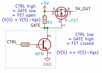 Here’s a simple FET circuit that lets you switch power to, say, a USB port, kind of like a valve that interrupts the current flow. This circuit uses a P-FET – to turn the power on, open the FET by bringing the GATE signal down to ground level, and to switch it off, close the FET by bringing the GATE back up, where the resistor holds it by default. If you want to control it from a 3.3 V MCU that can’t handle the high-side voltage on its pins, you can add a NPN transistor section as shown – this inverts the logic, making it into a more intuitive “high=on, low=off”, and, you no longer risk a GPIO!
This circuit is called a high-side switch – it enables you to toggle power to a device at will through a FET. It’s the most popular usecase for a FET, and if you’re wondering more about high-side switches, I highly recommend this brilliant article by our own [Bil Herd], where he shows you high-side switch basics in a simple and clear way. For this article, you can use this schematic as a reference of how FETs are typically used in a circuit.
Small Talk
There’s different kinds of FETs – MOSFETs, JFETs, and a few dozen less popular but still abundant ones. When talking about a FET, people usually mean a MOSFET, and that’s what this article is going to talk about, too – other types aren’t as popular for the usual hacker purposes, and I don’t know much about JFETs to begin with. They’re all field-effect transistors, however, siblings to the other kind of transistor that’s abundant – BJTs (Bipolar Junction Transistor), popular enough that we typically just refer to them as NPN or PNP transistors. These are all under the transistor umbrella, but when people say “transistor”, they usually mean BJT, and when people say “FET”, they usually mean “MOSFET”.
 You can imagine a FET as a resistor you can control, and its resistance can go as low as a fraction of an ohm (open), or to an infinitely high resistance for the purpose of your design (closed). You open the FET by charging and discharging its gate – at its simplest, you can imagine the gate as a capacitor. To sum it up, a FET is a transistor that acts as a resistor, with a built-in capacitor for controlling the FET’s resistance.
This makes FETs uniquely wonderful for things like power rail switching! When controlling a device’s power rail with a BJT, a voltage drop of at least 0.3 V is inevitable due to the way BJTs work – wasting power into heat as a result, and a no-go for digital devices where supply voltage matters. A FET in the same application, however, will just be an inline sub-ohm resistance – efficient and friendly. This is the main reason why FETs are used for power switching applications, and you will see FETs in all kinds of places as a result.
Now, a FET doesn’t instantly go from “fully open” to “fully closed” – just like with BJTs we all know and love, there are in-between states too, where resistance is not as low as the FET goes, but also not infinite – the FET is partially open, or, in other words, in its linear region. You can reach the linear region by applying an almost-open-but-not-quite kind of voltage to the gate, and by taking advantage of this, you can build an amplifier, an electronic load, or a constant-current driver for some LEDs. For switching purposes, however, a FET in the linear region is something you want to avoid – high resistance means high losses and the need to dissipate that heat somehow.
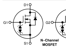
 Due to the way that FETs are built, each FET has a diode built-in, known as a “body diode”. You can’t avoid this diode – it’s there to stay; you can only account for its existence when wiring things up. If a diode is undesirable, a way to avoid it is by putting two FETs back-to-back. This is how LiIon battery protection circuits work – they need to protect the battery from overdischarge by shutting off the current that flows out, but they also need to protect from overcharge by shutting off the current that flows in, and putting two FETs in series with the diodes facing each other is one way to accomplish that. If you look at a higher-current LiIon battery BMS, you will inevitably find two FETs wired up like that, or even two rows of FETs put in parallel!
How does a FET actually work on a physical level, without the simplifications? Here’s a video from [Thomas Schwenke] on FETs specifically, and also one from [EEVblog] that talks about both BJTs and FETs. There are also myriad learning material and examples online, like this beautiful GIF from Wikipedia. You don’t exactly need to know this, but it might help, and it’s absolutely fascinating, too!
Opening Up
To open a FET, you need to apply a voltage to the gate that exceeds the FET’s Vgs threshold and doesn’t exceed the Vgs(max) value. Both of these are found in the datasheet, of course. Beware – Vgs in the datasheet (and online retailer part pickers!) is often given for some acceptable value of resistance, but not for the lowest resistance that the FET can achieve, so, you’ll want to check the Vgs-to-resistance graph in the datasheet. Now, in Vgs, G stands for gate and S stands for source – the third pin is drain; once the FET opens, current flows from source to drain. Of course, the gate control voltage has to be supplied relative to source, too.
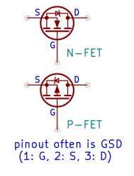 Just like with NPN and PNP transistors, there are N-FETs and P-FETs. N-FETs are like NPN transistors – the gate pin needs to have higher voltage than the source pin for the FET to open. P-FETs are like PNP transistors, too – the gate pin of a P-FET needs to have lower voltage than the source pin, of course, exceeding Vgs; in P-FET datasheets, Vgs is shown as a negative number, say, “-1.7 V”. As you might have noticed, it’s easiest to use P-FETs for high-side switching and N-FETs for low-side switching – as long as your Vgs is smaller than your power rail voltage, you don’t have to go outside of the range of voltages available within your circuit.
Now, when wiring a FET up, remember about the body diode – if you use a FET for load switching and wire it up the wrong way by mixing up source and drain, your device will always be powered through the body diode, no matter if the FET is open or not. On the other hand, checking with the datasheet for the pinout will eliminate this problem, and when drawing the schematic, the FET symbol will often have the diode drawn inside – or, at least, an arrow going from the same pin.
As for the naming, it’s easy to remember – when doing high-side switching with P-FETs or low-side switching with N-FETs, you connect your power source to the source pin, positive rail in case of a P-FET or the negative rail in case of an N-FET. Even if you need a FET for a different purpose, this particular mnemonic can remind you from which to which pin the body diode goes! P-FET, positive source. N-FET, negative source.
Once you got a FET, there’s a few ways to put it into a circuit. If you’re switching a 3.3 V power rail and your microcontroller is 3.3 V, you might as well drive the FET directly with a GPIO – while charging a FET’s gate isn’t always GPIO-friendly, gate capacitance won’t be much of a load on your GPIO at a small scale, so it’s a good shortcut in hacker projects; if concerned, you can add a series resistor between the gate and GPIO, say, 100 Ω. It’s also quite popular to drive low-side switching N-FETs with a GPIO, just like we do with NPN transistors!
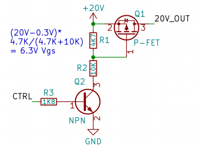
However, if your voltages don’t match, say, you’re controlling a 12 V load with a P-FET and a 3.3 V GPIO, there is another, way more popular way, that you’ve seen in our first example schematic – use another FET or BJT to pull the gate into one direction, and a resistor to pull it into another; if you need to keep your Vgs within a certain range, just add an extra resistor between the gate and the control transistor to form a voltage divider!
This is super useful, but not flawless. The gate is a capacitor, so charging or discharging it through a resistor will take more time than doing the opposite with a transistor, so the resistor-driven direction will spend more time in the linear region. This isn’t much of a problem for switching loads on and off occasionally, but it will bite you if you decide to do higher-frequency PWM – say, you’re driving LEDs or controlling speed of a motor, with the motor’s inductance messing things up even further. That’s where FET drivers come in – it’s a small chip that has a push-pull stage inside of it that helps you drive the gate strongly despite the capacitance, and keep Vgs within an acceptable range, too. More or less, connect your control GPIO to one side of the chip, your FET’s gate to another, follow the gate driver’s datasheet, and you’re golden.
Setting Boundaries
Of course, FETs have their limitations and nuances – there are myriad FETs in SOT23 packages that all look the same, but only some of them will keep up when you need to drive a few meters of an LED strip. The most important parameters are drain-source maximum current and voltage – these define the kind of load you can drive with a FET. If you want to drive a 12 V / 3 A load, it would be wise to pick a 20 V / 4 A Vds/Ids FETs, and if it’s a 3.3 V / 1 A, a 12 V / 3 A FET is the usual choice. Oh, and, the body diode might look extremely convenient, say, if you’re switching inductive loads, as it would dissipate some of the backwards EMF that the FET might get – don’t rely on it too much though, if you need a diode, adding an extra diode in parallel is a better way.
Have you found some nice and cheap FETs, or maybe you got some good ones in your stash, but they’re a bit short on the maximum current they can handle? Good news – you can often put similar FETs in parallel to increase the maximum current capacity! Unlike diodes, most FETs have a positive thermal coefficient – as more current flows through a FET and its temperature increases, its resistance increases too, which results in paralleled FETs balancing each other out – even if their parameters aren’t perfectly equal. You don’t even need to have separate driving circuits – just parallel FETs together, all three pins ganged, and it will work.
The gate pin is more touchy than the drain and source – for instance, it’s quite ESD-sensitive, and some FETs even have ESD protection diodes built in, wired between gate and source. Unlike with BJT transistors that need a constant current flow, you only need to charge a gate once for the FET to remain open for a fair bit – and it’s such a small amount of charge that you can often literally charge a FET’s gate by merely touching it with your finger, if the gate isn’t being actively pulled into any direction. See the R1 resistor in the intro circuit? It keeps the gate discharged and the FET closed unless it’s not actively being opened – without this resistor, the FET would not close on its own, and it would be susceptible to all sorts of noise. Unless you’re using a gate driver, you’ll absolutely want a gate-source resistor.
Also, generally, maximum Vgs threshold is way lower than Vds threshold – for instance, for a 30 V Vds FET, it’s not uncommon to see the maximum Vgs be 12 V or so; exceed it and the FET is quite likely to fail. Let’s say, you’re switching 20 V with such a P-FET, in the usual high-side switching configuration, and you get good Rds (drain-source resistance) at -6 V – you’ll want to keep the gate at about 12 V. Again, the easiest way to do that is a voltage divider, and the gate pull resistor will fit nicely into the picture!
 When a FET fails, it usually fails short-circuit – this is quite bad if you’re relying on the FET for anything critical, but if there is one upside, it’s that it is quite easy to debug when your FET has failed. Some products, like the Pinecil, use two FETs in series to further safeguard from such issues – indeed, having a soldering iron’s tip heat up uncontrollably is bad for your customers. Other products just use a single FET and don’t bother – failures are overall rare.
Speaking of the Pinecil, it uses an unorthodox driving circuit – it has an NPN transistor, but its base driven through a capacitor, so that only the AC component of the driving signal gets through. As a result, if the main MCU hangs and the control GPIO is stuck high, the FET won’t stay enabled!
Until Next Time
Would you like to learn more in-depth about FETs? There’s plenty of information online. For instance, this TI app note about driving FETs is wonderful. Over here at Hackaday, we’ve also taken a look at FETs in a few different contexts – CMOS logic, high voltage switching, part sourcing and general transistor wrangling, as well as covered a few introductory guides.
Of course, there’s way more fun things to learn about FETs! Next time, let’s move from schematic snippets to real-world uses – I want to show you a bunch of cool circuits that use FETs in perhaps less conventional ways; from reverse polarity protection to soft-start circuits and level-shifting, there’s a number of purposes that a FET could have on your board. Oh, and there will be part number recommendations, part picker tips, and some FET trivia that you might find useful for your hacking journeys and completing your FET mental map!


I initially struggled with the concepts of open and closed. In the end I thought of it as a tap rather than a switch
In some ways FETs (as well as IGBTs) are similar to goatse, it’s stretches and it’s never fully closed.
you kid, but
This is honestly a very rewarding click
Open and closed mixed up in text? Fraction of an ohm should be closed. Great write-up
travelling rn, can’t check.. isn’t “open” == “current can flow through”?
and thank you! ^~^
By convention, in the context of a switch or a relay, `open’ is off (the contacts are open in a mechanical switch- there is an open gap preventing current flow) and `closed’ is on (the gap is closed- current can flow). This has been followed in the transistor realm since they were first manufactured, when used as a relay or mechanical switch would be.
Your usage is the water valve usage. Having arrived at the end of the electron valve era, I never noticed which convention is used there in switching circuits, having used them mostly for analogue applications.
yeah, this is aimed at beginners more than people who already have an open/closed context like this. Fair point – I’ll go through the article and see if I can make an edit or two for clarity!
Well then it is critical to get these beginners off to a good start and properly educated. Probably using on/off rather than open/closed would make this clear or if you want to use a non-standard definition of “open/closed” for “clarity” (ahem).
You are then obliged to define your out of the ordinary use of said terms.
I went a different way about it given the context, and my assessment is that it will work out!
Especially since this is aimed at beginners, if you are using the terms “open” and “closed” then it is CRITICAL that you use them as they have been used in electricity and electronics for probably a century or more. Failing to do that will only cause confusion for beginners.
In a later comment you make an “assessment that it will all work out”. This is not the attitude of a responsible educator who takes the job seriously.
In response to these angry people, see my reply above for more detailed response, but don’t you see that the traditional open close terms do not actually apply here? There is no partially open switch or relay. It could be made clear that open/closed is not used in the traditional sense, but its not really even necessary, since those terms are used in a consistent way throughout the well written article.
While I agree with you in the context of a switch, where the two options are open or closed, but when you start getting into partially open or closed, I tend to agree with Arya on this one. You don’t think of a resistor being added in a circuit as a partially closed or open circuit, the circuit is fully closed, just not a short. Therefore, to describe a fet in the linear region, the analogy of a water tap seems to apply much more readily. Especially because, if you were to use the standard open vs closed terminology, it is actually somewhat indeterminate. Partially open doesn’t mean anything, because its a binary state. Either open or closed. Therefore, I agree with the valve analogy open/closed usage, although to avoid all of our pedantic discussions/outrage, the author could make a disclaimer about partially open referring to the fet as though it were a water tap and not the traditional switch terminology.
Arguments can be made for both. If you think of it as a switch, “open” means that the contacts are physically disconnected. That’s the more intuitive train of thought for people who are used to mechanical switches and relays. However, internally, a MOSFET operates by “pushing” electrons (or holes) away from the diffusion zone, forming a channel through which current can flow. This channel is said to be “open” when it is conducting.
oh aye! for me, “open”/”closed” is like a door – electronics can either pass through, or they can’t =D
It can still be like a door, but the electrons are going through the wall and trying to reach the wall on the other side!
Great article!
I have to disagree, I’m afraid. Every electrical/electronic engineer is familiar with the concept of open circuit and closed circuit.
Your use of open and closed doesn’t make it easier for newcomers to FETs, who will almost certainly have already encountered switches and relays. I think it will confuse them. And if it doesn’t confuse them when reading, it will definitely lead to confusion when they are talking to other people about the operation of FETs.
I’ve been doing electronics personally and professionally for over 45 years, and your nomenclature confused me.
Having said all that, your article is otherwise superb.
Yes. In electronics convention, when a switch is closed- circuited electric current can pass through it. When switch is open-circuited current cannot flow through it.
In French I wrote this years ago : https://connect.ed-diamond.com/Hackable/HK-012/Nos-amis-les-MOSFET (“our friends the MOSFET”)
The threshold voltage (Vth in datasheets) actually does have a mathematical definition, but in simple terms it’s the minimum voltage at which the FET will *begin* to conduct in its linear region. Basically it’s the point at which the channel starts to open. As such just meeting the Vth spec of a FET will generally not turn it on, especially over the full temperature range.
Trivia time – a fun thing that I couldn’t fit into the article! Remember the “don’t leave the gate floating, unless it’s driven by a gate driver IC” thing? In laptops, voltages are generated using a combination of a push-pull (one from VIN and one to GND) pair of FETs, and a step-down DC-DC controller with built-in FET gate drivers; the step-down chip (or the combination) is called a VRM. It’s a pretty good way to build a high-power step-down converter, especially when you need to produce 100A at 1V for the CPU! Nowadays, there’s even VRMs with built-in FETs in use – and becoming more and more popular!
Well, when a laptop breaks, sometimes it’s that one of the power rails shorts out, and sometimes it’s a rail that powers the VRM chip, or perhaps one of the FETs goes weird and you need to debug it – then, taking the VRM off is a tempting move. However, in laptop repair videos, you will often hear: “don’t power the laptop on with the VRM IC desoldered!” And that’s for a good reason – if you do that, you leave the FET gates floating, and the FET that goes from VIN to the step-down output, might just open and attempt to power your soldered-on CPU or RAM with 20V – which tends to end badly 😅
Oh, and something I wanted to add but forgot – there are enhancement and depletion FETs. Generally, you will only see enhancement FETs – depletion FETs are quite rare. The difference is – enhancement FETs are closed when their Vgs is 0 (you have to apply Vgs to open the FET) – the article assumes an enhancement FET. Depletion FETs, on the other hand, are open when their Vgs are 0 *or* Vgs is applied – to close a depletion FET, you have to actively drive Vgs into the opposite direction, as in, lower than Vs for N-FETs, and higher than Vs for P-FETs.
Quite rare – unless you happen to be getting into silicon design!
(In which case you’re probably not needing to read a HaD article to figure out what’s going on, but still)
Some small-signal MOSFETs and most small-signal JFETs do not have body diodes. For example, the MFE3002 MOSFET and the BF510 JFET.
I wonder why all load switching devices i came accross, like USB/Ethernet controlled power strips or remote controlled power outlet, use standard (non latching) electromagnetic relays instead of FETs? These relays require a constant power to be applied to maintain the relay closed and the load powered on, so much more power loss than with FET.
Oh, good question! Generally, relays and and triacs are used because they’re the easiest, least lossy when it comes to contact resistance, and tick all the “control anything” boxes, ie providing good isolation! Switching AC with a FET is doable, some SSRs will use FETs internally, but a relay is just the tried&true solution, and I’d bet it’s cheaper. My guess is that designers of power strips don’t bother improving the user-end power consumption to such an extent – they’re the one on the hook for the extra cost of an SSR, but when using a relay, end users pay for the electricity wasted =D Also, IIRC, the power spent on holding the relay closed, isn’t all *that* much in the grand scheme of things.
1. Relays are simple and cheap.
2. Fast switching isn’t necessary.
3. Relays provide galvanic isolation (this is a must for mains)
A single MOSFET can be configured as a switch, but keep in mind that high power MOSFETs become physically large (and expensive). Driving large MOSFETs also becomes complicated as you sometimes need gate voltages that exceed whatever voltage you are switching. What you are actually describing is a solid state relay. Those usually have several stages, and are generally optically isolated as well.
It’s amazing that your average cheap SSR can be less efficient than your average cheap relay for AC, after all these years of development, the century(?) old tech is still relevant.
What I still don’t understand is why we switch DC with anything other than smart switch ICs with the built in overload protection and diagnostics. Surely we could make them for a few cents if we made as many of them as we do relays, right? But I suppose that kind of change takes time and the clicky sound is pretty awesome.
Thanks for enlightening me !
Small relays are not really cheaper (by themselves) last time I looked but when switching AC control voltages (often 24V AC in US) or mains they are more forgiving of wild spikes and noise I think. Back when digital thermostats (for home heating units) were first exploding on the scene I was soon seing expensive control units “burning up” which traced back to a pretty high failure rate of the triac failing in what I call “high impedance mode” i.e. not off enough and/or not on enough. It is still rare to walk by a state of the art Heat Pump/furnace control or thermostat that doesn’t make that “click” of the small relay as it engages..
Galvanic insulation, among other things. An electro-mechanical relay can be driven by a separate power source, if required. You can savely use a 5v DC relay to switch on/off a AC mains power, provided that the relay contacts can handle the current that flows.
Fun fact: depending on how you look at it, BJTs are actually more efficient. It boils down to semiconductor physics that I am not ready to explain, but BJTs tend to have higher gain and at very high voltages they can maintain a low voltage drop between base and emitter, something that MOSFETs can’t match with their resistive channels. This is the reason IGBTs (insulated gate bipolar transistor, basically a MOSFET driving a BJT) exist.
Because a BJT always drops 0,3V regardless of applied V but a FET’s voltage drop rises with the applied voltage (it’s R is constant, not the voltage drop)?
^^ real question. I’m not much of an electronics nerd on that level…
Yep, that’s the idea. Mosfets are better at low voltage high current, and btjs or igbts are better at high voltage. (better in regards to power loss / thermal heating)
At very low currents both the base-emitter voltage and the collector-emitter voltage can get very close to zero. A 10 millivolt collector-emmitter voltage is not unheard of in some obscure audio chopper circuits. The base-emitter voltage is a logarithmic function of the base current.
Great article!
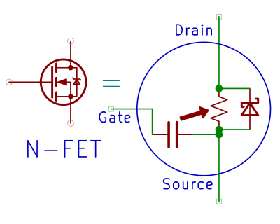
For following along, it would help if the image with the N and P-FET included labels for gate, drain and source.
yes! right, that’s one another thing I was about to do, but then forgot last minute! lemme fix that real quick
JFETs are remarkably similar to triode valves. Current normally flows, and a bias voltage on the grid/ gate will turn them off.
I have heard valves described as FETs with a pilot light – or an afterburner (if you want high voltage).
And the FET is indeed a (at least virtual) contemporary of the tube age – long before the bipolar transistor was invented in 1948 ;-)
https://en.wikipedia.org/wiki/Field-effect_transistor
The vo-tech I attended in the latter 1970s, first taught us vacuum tube theory, then JFETs, then BJTs.
That was wise, I think.
If you learn it the other way round, with that weird water pipe analogy of BJTs, you will have a heard time understanding the real working of thermionic valves and transistors.
Same can be said about programming, maybe.
Those who learnt proper programming with Pascal first (Turbo Pascal; Turbo Basic/Quick Basic also had Pascal elements to be fair) do struggle less if being asked to write in plain BASIC or C later on than the other way round.
Anyone else not remember what is different about a jfet and get a little let down that we were almost told, but got shut down? Just a curiosity tease
The vulnerability to static?
(Sorry for that, I genuinely don’t know, and didn’t want to spend yalls time with a rehashed explanation I would’ve had googled! =D )
Oh, it’s just that way back in the olden days, FETs were shipped with a shorting ring to keep all the leads at the same potential. The shorting ring was not removed until the FET was soldered into place.
Then antistatic foam was invented and FETs were designed with Zener diodes between the leads to suppress damaging transients.
Sometimes they were wrapped in alum[i]um foil to protect them from transients.
They were touchy little boogers.
You’re talking MOSFETs. They arrived and the first thing you learned about them was static protection. They were fine in circuit, but untilthen nothing to dissipate any static. By the time I got some about 1972, they had the protection diodes.
But people fuss about JFETs. I was never sure if I mssed some detail or people were conflating the two. I certainly never heard worry until about 1990.
On th other hand, if you had one as the input stage to a shortwave receiver with a long wire antenna, that’s a different case.
Long story short — it’s just a NOT-gate (and the output is buffered).
MOSFETs work in small-scale in solar/battery apps, we find.
Have lots charge/load controllers at <~$20 used with 100 W poly/monocrystalline <$100 solar panels used to power Raspberry Pi 4Bs.
MOSFETs work well to eliminate erratic and intermittent solar panel electric power output, we find too.
No Pi 4B power resets.
Can MOSFETs work with huge batteries on grid-scale RE solar/wind systems?
JFETs are basically a variable resistor. The Gate lead is the cathode of a diode, whose anode is the Source lead. The JFET has low resistance when this diode has 0 volts across it.
The JFET’s resistance goes up when the Gate diode is reverse-biased (goes negative with respect to the Source lead). If the gate voltage goes negative enough to reach the pinch-off voltage, the JFET source-to-drain becomes an open circuit.
Since the gate is basically a diode, JFETs are generally not susceptible to static (no more so than the base-emitter junction of small-signal bipolar transistors).
One interesting feature of JFETs is that in many cases the Source and Drain leads are interchangeable. There is no body diode as there is in a MOSFET. JFETs thus make good analog switches, since they carry current in either direction when on, and block current in both directions when off (where ‘on’ means conducting, and ‘off’ means not conducting).
Oh, and then there’s the NixonFET. It has a water Gate, an unimpeachable Source, and financial Drain. :-)
Personally, I would *never* use the term FET when I was talking about a MOSFET or a JFET. I use both extensively, and mainly (but not exclusively) for RF. “Hackers” may use just FET, but I don’t see why. FET may be slightly more specific than “transistor,” but why be vague–or use slang–when it’s just as easy to be precise? Even odder are those who use “transistor” when they mean a BJT but then some form of FET (and not “transistor”) when referring to those. It like saying “meat” for beef (but not chicken), or “metal” for steel (but not aluminum).
It’s worth noting, for instance, that MOSFET gates can be ESD sensitive, but those of JFETs aren’t, or at least not any more than BJTs. Unlike the metal-oxide insulation of a MOSFET gate, the junction of a JFET will recover from ordinary-level ESD just like that of a BJT. Also because of the oxide layer, MOSFETs usually have a much-higher gate impedance than JFETs (which have much greater gate impedance than the “base” of a BJT. If you just say FET, these useful distinctions are lost in the weeds of sloppy usage.
Unfortunately your blog seems to be gone. I’ll ask here in case you see the question: JFETs are often better for the input stages of a radio receiver, compared to BJTs, because of their higher impedance. Why not use MOSFETs instead of JFETs, since they have even higher impedance?
I thought it was because BJTs have “shot noise”, FETs are quieter for amplifying weak signals in the RF stage(s).
I think you’re right.
As Ren points out, I don’t think it’s the high impedance that makes JFETs useful in RF front ends. It’s that they’re quieter than BJTs. A BJT in a common-collector/emitter-follower configuration can have pretty-high impedance too, but the BJT’s current-dependent junctions result in more noise than voltage-controlled JFETs. Small-signal dual-gate MOSFETs (sometimes called MOSFET tetrodes) *are* useful in RF applications as mixers and for gain control. Some power MOSFETs can be used for transmitting final amps, but only if they have relatively-low input and output capacitance (maybe <200pF), otherwise gain will suffer as frequency increases. Their main value is that they're very cheap. Example: IRF510 (≈$1).
This seems to me, this turned into a, which came first, the chicken or the egg debate.
The way I read the article was that the body diode is intrinsic to the FET’s junction. Is that incorrect?