
CMOS opened the door for many if not most of the properties needed for today’s highly integrated circuits and low power portable and mobile devices. This really couldn’t happen until the speeds and current drive capabilities of CMOS caught up to the other technologies, but catch up they did.
Nowadays CMOS Small Scale Integration (SSI) logic families, I.E. the gates used in external logic, offer very fast speeds and high current drive capability as well as supporting the low voltages found in modern designs. Likewise the Very Large Scale Integration (VLSI) designs, or Very Very Large Scale if you like counting the letter V when talking, are possible due to low power dissipation as well as other factors.
How CMOS is Designed
CMOS, which means Complementary Metal Oxide Semiconductor, is based on combining two polarities of MOSFETS; Metal Oxide Semiconductor Field Effect Transistors.
 Regular transistors, known as Bipolar Junction Transistors (BJT) meaning that they are made from junctions that have a positive and a negative (PN) junction utilize current as the input and create gain by controlling output current. As all of these current flows add up it means that at the end of the day there is a lot of current flowing which results in power being dissipated which ultimately results in heat.
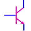
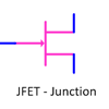 The Junction Field Effect Transistor (JFET) utilizes voltage instead of current on its Gate input, somewhat like the Base on a Bipolar Transistor, to control the output voltage. Since the Gate is not insulated from the other terminals, known as the Source and Drain, there is a leakage current in JFETs that would not be present if the Gate was insulated from the Source and Drain.
Enter the Insulated Gate FET (IGFET) which is the basis for most of the transistor devices found on large scale integrated chips today. Looking at the diagram, the MOSFETs all show a distinct space between the Gate and the rest of the structure. The other two pins are the Source and the Drain.
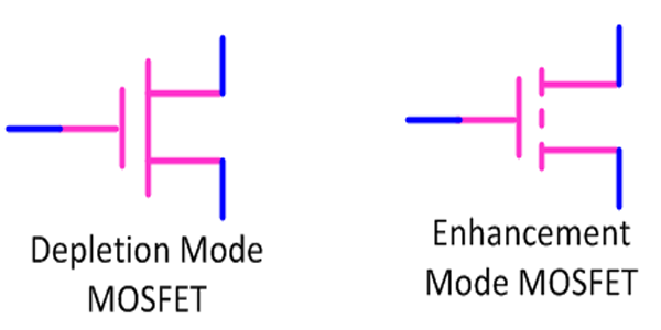
This is a real gap created by silicon dioxide, the “Oxide” in MOSFET. If that sounds like glass, a really good insulator, I would say well yes it is. If a good insulator sounds like a dielectric, the makings of a capacitor, I would also say that well yes, it is. FET’s come in two major modes of which there are two different types based on polarity. The major modes are Enhancement and Depletion.
An enhancement MOSFET needs a voltage applied to a gate for the device to turn on, it can be thought of as a normally closed switch as opposed to a depletion mode device which needs a gate voltage applied to turn off and can be thought of as a normally open switch.
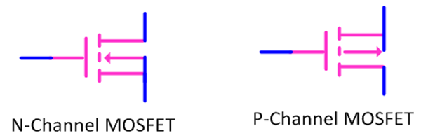
FET’s come in two different polarities based in part upon the polarity of the Gate signal and how it affects the device: An N-Channel device is activated when a positive voltage is applied to the Gate compared to the Source and a P-Channel activates with a negative voltage.


By combining an N-Channel device and a P-Channel MOSFETs an inverter is implemented. When the Gate is High the N-Channel MOSFET turns on pulling the output Low. Likewise when the Gate is Low, the P-Channel MOSFET is turned on pulling the output High. Note the alternate way to draw the MOSFETs on the right that is a tad more intuitive as the bubble on the P-Channel indicates that a Low on its Gate will turn it on.
Unprotected CMOS Can Be Fragile
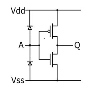
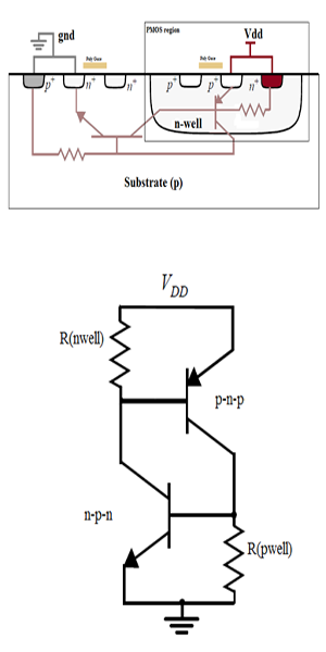 The High Impedance on the input, I.E. the lack of a load resistance to a ground, means that a little bit of static charge on something like the human finger, can actually be disastrous for an unprotected CMOS circuit. A simple spark or otherwise invisible charge can ruin a MOS based device by punching holes in the gate insulation. Another problem caused by excessive voltage is what is called “SCR Latchup”, basically an excessive voltage causes the PNPN junctions produced by layout to act as back to back transistors that cascade into full conduction resulting in a short circuit between power rails. The only way to relieve the shorted condition is to remove power from the device which allows all of the energized transistors to turn off. The addition of protection diodes as shown is pretty standard across the board, though sometimes the diode function is really implemented with on board JFETs.
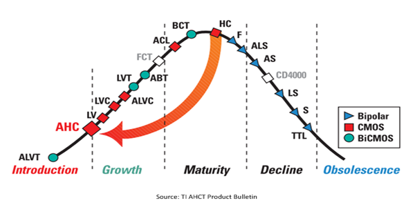
Let’s talk about CMOS logic families. The table below shows the curve between the newest families and obsolescence. Many of the comments on the video on TTL properties mentioned that TTL is for the most part “mature”, old, and/or obsolete. While this may be true in general, the legacy of TTL logic levels lives on in the form of TTL compatible families, usually denoted by a “T” in the family name.
CMOS vs. TTL
The voltage levels of CMOS based logic are somewhat different from TTL, basically instead of the preset levels of Low(.4-.8v) and Hi(2-2.4v) the input logic levels of CMOS are mostly expressed as a ratio of the supple voltage.
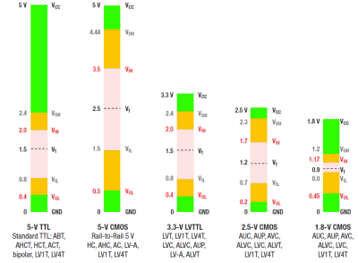
The output voltages are usually within a few tenths of volts of each rail and the input thresholds are generally 1/3 and 2/3 of the supply voltage for Low and High respectively. This has the effect of maximizing the noise margin as the near rail-to-rail output swing (from near ground to near the power supply) ensures that the gate has the maximum output voltage swing.
It’s important to note the CMOS works best and uses the least power when the gates are turned all of the way on or all of the way off, it is very important that the voltage be kept out of the area shown in pink on the table.
CMOS outputs can generally connect to TTL inputs providing that the CMOS output can supply enough current. Feeding a CMOS input from a TTL output is a bit more problematic as the TTL output of 2.4V in a 5 volt system is not high enough to guarantee a High is seen by the CMOS part. Generally a pullup resistor can supply the last little bit of voltage but a cleaner approach is to use a “T” type CMOS part such as an HCT instead of HC, or a AHCT instead of AHC.

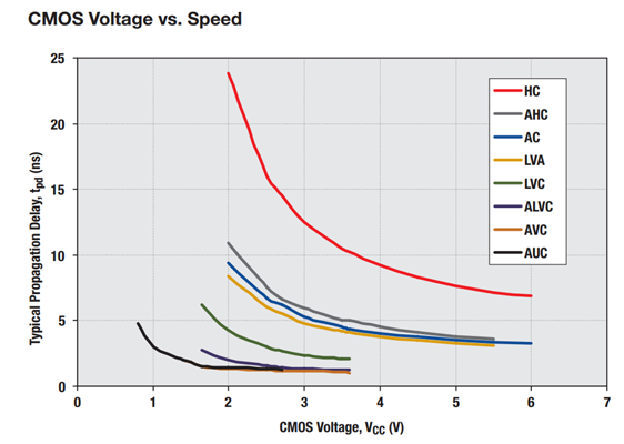
Low Voltage and High Speed
The chart below shows the migration CMOS has made over the years as it increased speed and ultimately support for the lower voltages; down to 0.8V as shown. The technology trend ends up with older families in the upper right, the newer and more advanced families down in the lower left. During this time other attributes also improved including output current with 24-60ma drive current becoming not uncommon. Low voltage and higher speed do tend to go hand in hand as the voltage has less “distance” to slew. With the new voltages come some other issues such as translating between them which I will cover just a bit in the next post.
Next Time
In the next video I will show some CMOS logic family capabilities that include supply voltage translation such a 3.3v to 5v and also including down to 0.8v, a bus “hold” function, and will try my hand at showing how to lay out a CMOS gate and what some of the various layers and technologies are that are used in CMOS fabrication.
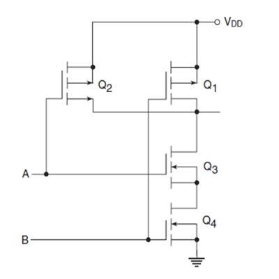
For your quiz this week, what logic function does the following drawing depict :


LOL @ the quiz in the end! It already contains the answer :-)
I had to triple check because I thought it might be some sort of trick! :-)
Yeap, I’ve done the combinations in my head too, just to validate the answer. I am a little rusty due to being in software development for the last 10 years instead of doing electronics engineering as I was supposed to.
Haha… very observant. Fixed.
No problem since I had to do the combinations to validate that the written answer was right, although the depicted example is a common one in many CMOS design textbooks as it is a basic building block for CMOS based ICs.
I will post the circuit the chip guys would use when they interviewed new candidates when I get a chance. :)
Please do post it. :-)
Lol… just one of my symptoms of being an olde burnout. :)
What I should have added to the question was to ask HOW does it work as the pulldowns in series demonstrates something cool that can be done with FETs, at the end of the day they both see similar Gate-to-Source voltages resulting in them both turning all of the way on.
Nice tutorial! More quizzes please!
Is it the ability of a FET to sense its own output on its input that gives it the reputation of being noisier than JFETs and BJTs?
I assume you’re talking about a MOSFET. They have a very high input impedance, and therefore they pick up noise more easily than JFETs and BJTs, which have a lower imput impedance, because they require far more current in order to switch. (The MOSFET in theory doesn’t have any input current, but in reality they have a bit of leakage). So if the driving circuit around the input is also high impedance, then it picks up noise easily.
Sensing it’s input can happen if large voltages/currents are driven at the output, which can be coupled back to the input.
Trying to find the right words I would say that the high impedance if the IGFET, especially when used as an amplifier,loads down the signals, and noise, (MUCH) less and can give a more accurate picture in general, including noise sources. Also when talking about high frequency noise less resistive load means that there is less of an RC low pass filter going on where the capacitance is any intentional or unintentional capacitance present.
With that said a proportion of the capacitive load on the output can be “felt” on the gate which increases the current required to charge those capacitances which can become a source of noise also.
You guys seem to be saying about the same thing…
So to confirm, a power MOSFET with low voltage and high current isn’t more susceptible to oscillation in spite of its higher capacitance, because the capacitive load on the output can’t be very big? Conversely, a high-voltage MOSFET with a low capacitance isn’t going to oscillate unless you leave very long legs on it?
Well I will start by saying noise and oscillation are two different things. From there the rest is entirely dependent on the circuit design and implementation and the more aggressive the design the more careful the designer has to be. The simplest axiom is that for oscillation to occur there needs to feedback and phase shift. If the device driving the FET isn’t stable with a capacitive load and it sees a capacitive load then that would be one simple example of a problem. I keep the book Switching Power Supplies A-Z by Maniktala in my bathroom and it is an excellent source on power FET use and problems.
If you look at the time on the replies we both replied at the same time! :)
“The simplest axiom is that for oscillation to occur there needs to feedback and phase shift”
That is elegant. Thank-you.
I do IC layout for a living. Cool to see some cmos stuff show up on HAD.
I was thinking about actually firing up a copy of Magic or something similar and laying something out in the next Vid. Or I might fake it with Visio depending on time. >:)
That’d be really cool. I’ve never used magic. May have to check it out. I’ve used klayout as a viewer but I believe it’s capable of drawing as well. Everything I do on the daily is done using cadence (aka the evil empire).
Cadence, Mentor….. We used to use Calma.
We used Cadence in Uni. Silicon Ensemble, Virtuoso, NVHDL are some of the tools that we’ve learned. Unfortunately, I haven’t touched these since the uni times :-(
Those with Fran were more funny.
I will let her know. :) Here the format doesn’t give me much time to breathe let alone banter. ;)
Vaguely related game about fab that popped up a while back. http://www.zachtronics.com/kohctpyktop-engineer-of-the-people/
Nicely done. I found it a nice refresher and it was good to catch up on the newer technology. I started tinkering in electronics in the ’80s, when the main choices were 74xx, 74Fxx, and 74LSxx.
I also want to compliment you on your writing. It is easy to read, and shows your competence in the subject matter with a touch of modesty; you don’t come across as lecturing or talking down to your readers like some others do.
Thanks!. I consider myself luck if I can make my way through a post without suffering a bizarre related keyboard injury.
I think you’ve got a typo up top referring to an enhancement mode FET as normally closed and depletion mode as normally open. Isn’t it really the other way around?
I saw that too. Enhancement should be normally open (off) and depletion should be normally closed (on).
crap carp carp crap….. I proffed it a dozen times.
Hopefully the video is right, that’s really where i out my effort and the post is a tease.
BTW, the video is accurate, and very good. I usually just read the articles on account of being at work. I’m learnin’ stuff at work! That never happens.
Once again, a seasoned professional with a storied career is bested by an ignoramus using Wikipedia! I mean, you know, on one typo. Not career-wise.
I’m not sure about which one of them is using Wikipedia.
He also is way off kilter in saying the two types, E and D, are differentiated by polarity. Um, no. E & D are strictly defined by pinch-off voltage.
NFET and PFET are based on polarity.
I like the way Bill brings in real life experiences, this is very interesting. I personally learned a lot from the book “CMOS VLSI Design: A Circuits and Systems Perspective” which I can absolutely recommend.
Maybe you should also brought in some words about the correlation between the pull up and pull down networks for logic functions in cmos.This way the quiz would also have a teaching effect ;)
An even better teaching effect. Sorry ;)
I think I will, thanks. Its a complicated subject that sounds simple and then there is the use of depletion mode devices (on till shut off) . I used to say there is no such thing as a pull down which can tend to piss people off.
It is a complex subject indeed. If the reader is new to transistors I guess it will take some time to get through the article. For the others it’s a nice refresher plus some extra info.
Whats wrong with pull-down? (I am not pissed off, only curious)
Could someone please give the answer to the quizz and explain? I’m new to MOSFETs so I tried but couldn’t find a truth table that makes sense…
It’s a NAND or not AND if you like. It’s an inverted AND gate which I’ve always thought was interesting because it doesn’t have an inverter in it, but the AND gate does.
Truth table.
AB out
00 1
01 1
10 1
11 0
Little History on CMOS and a company that amazingly survived for over 40 years in the Semiconductor World.
http://www.fundinguniverse.com/company-histories/standard-microsystems-corporation-history/
There is something wrong with this phrase in the article:
“…An enhancement MOSFET needs a voltage applied to a gate for the device to turn on, it can be thought of as a normally closed switch as opposed to a depletion mode device which needs a gate voltage applied to turn off and can be thought of as a normally open switch…”
‘Closed switch’ – means the switch conducts but in the passage above ‘closed switch’ implies that it does not conduct.
Same problem with the usage of ‘open switch’.
An informative article otherwise.
Thanks for reading the post 5 days prior that is pretty much what you posted
It’s interesting to know this stuff and I agree with the comment above regarding life experiences.
Do people use discrete logic chips anymore? Like a quad nand gate. Why?
Because they need it
Some are also magical
“Some are also magical”
Are those the ones with the magic smoke inside?