
Over the recent weeks here at Hackaday, we’ve been taking a look at the humble transistor. In a series whose impetus came from a friend musing upon his students arriving with highly developed knowledge of microcontrollers but little of basic electronic circuitry, we’ve examined the bipolar transistor in all its configurations. It would however be improper to round off the series without also admitting that bipolar transistors are only part of the story. There is another family of transistors which have analogous circuit configurations to their bipolar cousins but work in a completely different way: the Field Effect Transistors, or FETs.
In a way it’s less pertinent to look at FETs in the way we did bipolar transistors, because while they are very interesting devices that power much of what you will do with electronics, you will encounter them as discrete components surprisingly rarely. Every CMOS device you deal with relies on FETs for its operation and every high-quality op-amp you throw a signal at will do so through a FET input, but these FETs are buried inside the chip and you’d be hard-pressed to know they were there if we hadn’t told you. You’d use a FET if you needed a high-impedance audio preamp or a low-noise RF amplifier, and FETs are a good choice for high-current switching applications, but sadly you will probably never have a pile of general-purpose FETs in the way you will their bipolar equivalents.
That said, the FET is a fascinating device. Join us as we take an in-depth look at their operation, and how and where you might use one.
FET basics
A basic FET has three terminals, a source (the source of electrons), a gate (the control terminal), and a drain (where electrons leave the device). These are analogous to the terminals on a bipolar transistor, in that the source fulfills a similar role to the emitter, the gate to the base, and the drain to the collector. Thus the three basic bipolar transistor circuit configurations have equivalents with a FET; common-emitter becomes common-source, common-base becomes common-gate, and an emitter follower becomes a source follower. It is dangerous to stretch the analogy between bipolar transistors and FETs too far, though, because of their different mode of operation. A closer similarity exists between a FET and a triode tube, if that helps.
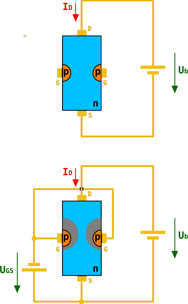
The simplest FET for demonstration purposes has a piece of N-type semiconductor with source and drain connections at opposite ends, and a zone of P-type semiconductor deposited in its middle. This is referred to as an N-channel junction FET or JFET, because the channel through which current flows is N-type semiconductor, and because a diode junction exists between gate and channel. There are equivalent P-channel devices, just as there are PNP and NPN bipolar transistors.
Were you to bias an n-channel JFET as you would a bipolar transistor with a positive bias on its gate, the diode between gate and source would conduct, and the transistor would remain a diode with two cathode terminals. If however you give the gate a negative bias compared to the source, the diode becomes reverse-biased, and no current to speak of flows in the gate.
A characteristic of a reverse-biased diode is that it has a depletion zone between anode and cathode, an area in which there are no electrons. This is what causes the diode to no longer conduct, and the size of the depletion zone depends upon the size of the electric field that exists across it. If you’ve ever used a varicap diode, the capacitance between the two sides of this variable-width zone is the property you are exploiting.
In a FET, the depletion zone stretches from the gate region into the channel, and since its size can be adjusted by the gate voltage it can be used to “pinch” the remaining conductive region within the channel. Thus the area through which electrons can flow is controlled by the gate voltage, and thus the current that flows between drain and source is proportional to the gate voltage. We have an amplifier.
![A simple FET radio receiver circuit showing FET biasing. The gate is biased at ground potential through the inductor, and the source is held above ground by the current in the 5K resistor. Herbertweidner [Public domain].](https://hackaday.com/wp-content/uploads/2018/06/1kreiser_mit_fet.png)
MOSFETs, where the FET becomes more useful
![Internal structure of an N-channel MOSFET. Fred the Oyster [Public domain].](https://hackaday.com/wp-content/uploads/2018/04/n-channel_mosfet-svg1.png)
Why would you use a FET?
So we’ve described the FET, and noted that while its mode of operation is different to that of a bipolar transistor it does a substantially similar job. Why would we use a FET then, what advantages does it offer us? The answer comes from the gate being insulated either by a depletion region in a JFET or by an insulating layer in a MOSFET. A FET is a voltage amplifier rather than a current amplifier, its input impedance is many orders higher than that of a bipolar transistor, and thus you will find FETs used in many applications that require a high impedance small-signal amplifier. The input of a high-performance op-amp will almost certainly be a FET, for example.
The high input impedance has another effect less coupled to small signal work. Where a bipolar transistor requires significant base current to turn itself on, the corresponding FET requires almost none. Thus almost all complex integrated circuit logic devices are FET-based rather than bipolar because of the huge power saving that can be made by not needing to supply the base current demands of many thousands of bipolar transistors.
The same effect influences the choice of FETs for power switching, while a bipolar transistor’s base current is proportional to its collector current and thus it will need a significant driver, by contrast a power MOSFET requires virtually no standing gate current after an initial surge. A MOSFET power switch can thus be built requiring much less in the way of drive electronics and much more efficiently than a corresponding bipolar switch, and makes possible some of the tiny driver boards you might be used to for driving motors in your 3D printer, or your multirotor.
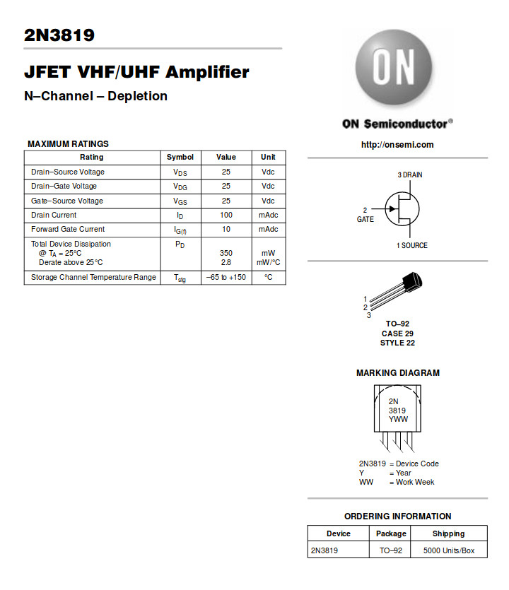
Through the course of this series you should have acquired a solid grounding in basic bipolar transistor principles, and now you should be able to add FETs to that knowledge base. We suggested you buy a bag of 2N3904s to experiment with in one of the previous articles, can we now suggest you do the same with a bag of 2N3819s?


” A closer similarity exists between a FET and a triode tube, if that helps.”
My Vo-Tech first taught us Vacuum Tube (Valves -Jenny) Theory followed by FET operation, and then we learned BJT’s, and other semiconductor devices. (well, I don’t recall, I’m sure semiconductor diodes came before FETs)
Continue reading —>
+1
Now just imagine if those diagrams were interactive?
Everything is interactive through imagination!
Ironically, that half-bridge was something I recreated independently rather early on. I needed to turn a TTL square wave into a +/- 12v square wave for my EVSE projects. I wound up using a pair of complimentary MOSFET arrays. The first array turned the TTL into two turn-on channels that would operate the second two MOSFETs to generate the output. It took a lot of iteration to figure it out, but in the end it works really well. https://hackaday.io/project/3939-j1772-hydra
Sounds like a good place to use a RS232 line driver.
++1 , Or an op-amp.
Two MOSFET arrays are a fuck-ton cheaper.
Why recommend a 2N3819 instead of something like 2N7000? Not only is the 2N7000 a MOSFET (which I’d argue is more common and more forgiving than a JFET), but digikey tells me that the 2N3819 is obsolete: https://www.digikey.com/products/en?keywords=2N3819
For small-signal mosfet work, the 2N7000 and BSS138 are good nmos choices. The BSS84 is a good small-signal P-mosfet.
For a starter kit of jfets, my personal choice would be the 2N4091-2N4092-2N4093 series.
Depletion-mode fets have different applications than enhancement-mode transistors, and it’s easier to design with them if you abandon the idea of plugging them into the standard BJT circuits.
As a simple example, a jfet with its gate tied to a fixed voltage makes a primitive voltage regulator. The relatively low transconductance means the gate-source voltage doesn’t change much for 5:1 variations in drain-source current, and is nearly independent of the drain voltage. As long as the current doesn’t change too much, the source voltage stays reasonably constant across a wide range of drain voltages. A TL431 voltage reference biased by a 2N4092 has phenomenal supply-voltage rejection.
Jfet series like the2N4091/2/3 are designed to have different Vgs voltages at the same current. At 1mA and with the gate tied to GND, a 2N4091’s source voltage will be 5V-7V, a 2N4092’s source voltage will be 3V-4V, and a 2N4093’s source voltage will be 1.5V-2V. Putting a 2N4091 above a 2N4092-TL431 makes the supply-voltage rejection practically infinite.
Depletion-mode jfets are also the magic component in attractive BJT circuits like an NPN current reference biased by a PNP current mirror. The all-BJT circuit is bistable: it produces constant current if all the BJTs are turned on, but does nothing if all the BJTs are turned off. Tossing in a jfet gives you a current path guaranteed to turn everything on, but doesn’t waste current or vary with the supply voltage once things are running.
BJTs and depletion-mode fets play to each other’s strengths. It’s a shame that jfets have fallen out of fashion.
Could you explain how to put a 2n4092 ‘above’ a TL431? I’ve looked at the datasheet and they do have examples with BJTs. Perhaps tying the gate to the anode of the TL431, and putting a resistor between the anode of the TL431 and the source of the 2n4092?
@mblytheter The real answer is that [Jenny] is a bit of a radio nerd, and that JFET is more of a radio part.
Honestly, I thought the same as you, though. I use MOSFETs to switch power more than I use JFETs as linear amplifiers.
And I used to use 2N7000s by the handful until I moved the voltage of most all of my projects down to 3.3 V – 3.6 V, where the 2N7000 doesn’t really fully turn on reliably. I need to shop around for a good substitute for general purposes.
I even wrote about it, and the comments are full of great suggestions. https://hackaday.com/2016/12/13/ask-hackaday-dude-wheres-my-mosfet/
“Not only is the 2N7000 a MOSFET (which I’d argue is more common and more forgiving than a JFET)”
You can easily destroy a 2N7000 just by touching it with bare hands, while a 2N3819 or any similar JFET will sustain much worse treatment. As a 2N3819 substitute, look for BF256. Not 100% identical (it’s more of a BF244 replacement) but very very close for non critical applications and still available in TO92 casing.
“you will encounter them as discrete components surprisingly rarely”
Not if you work with power electronics. The FET is the workhorse there. There’s a good change any switchmode power converter you have for a mains-connected device has one or more discrete FET devices.
Likewise all of my work driving lots of LEDs, thermostatically controlling heaters, gating power to subsystems, and amplifying RF to anything beyond a few milliwatts. MOSFETs are my first thought when I hear the word “transistor,” and BJTs have become something of a historical curiosity as far as my projects are concerned (though I still have that bag of 2N3904s, 2N3906s, and PN2222s hanging around).
in this case “FET” is referring to JFETs…you are talking about MOSFETs. I’ve never encountered a JFET outside of small signal stuff.
And that hybrid mystery, the IGBT.
IGBT is a small MOSFET driving large BJT. It’s quite a similar thing to Darlington circuit, where a small BJT drives a large BJT. Nothing mysterious about it :)
Also worth mentioning I think, in the ‘Why use a FET?’ category: they are thermally stable devices, and thus when used in situations that can generate lots of heat (eg: power amplifiers), tend not to stop and catch fire, unlike Bipolar transistors, which typically need additional protection circuits to achieve this. Details randomly selected from the ‘net here: https://www.quora.com/Why-FET-is-thermally-stable-than-BJT
isn’t a FET a voltage controlled current limiter with dependencies on temperature? I’d say ” FET is a voltage amplifier rather than a current amplifier” is absolutely wrong
Finally someone with my way of thinking – call these device amplifiers stumped me when I was learning first, what kind of magic is inside that makes them put out more than they get in?? Its obivious that they are just voltage controlled voltage limiters, and BJT’s are current controlled current limiters- as you cannot get more out than you put in at the input.
When do we get that machine that stabs people over the internet?
Please. A FET is not a voltage amplifier. A FET is a transconductance amplifier.
JFETs are using as the first active device in many many oscilloscope front-ends I’ve seen, as source-follower (impedance adapter). They have very high input resistance and very low input capacitance, 2 highly desirable characteristics on a scope’s front-end.
Well written. But “Schmidt buffers”? Are you sure of that spelling?
I’ve been doing this electricity stuff for longer than you’ve been alive, probably; and starting way before Electrical Engineering school–and through seven years of it–I’ve seen it spelt (that’s a good spelling, by the way, particularly if you’re of the British persuasion) as ‘Shmitt’, ‘Schmitt’, ‘Schmidt’, ‘Schmidtt’, and any other way which might drive the grammar and spelling Nazis nuts.
Major clue: it doesn’t matter.
Stay focused–and NOT ‘FOCUSSED–on the important stuff.
[The really important stuff includes NOT putting an apostrophe before the “s” in every word which ends in “s”‘ simply because it ends in “s”]
Stay focused.
“Besides a mathematical inclination, an exceptionally good mastery of one’s native tongue is the most vital asset of a competent programmer.” –Edsger Djikstra
Only if you are working towards your first century. I’ve been working with electronics and things since I was maybe 9 or 10 years of age, and been exploring the whole semiconductor scene since then as well.
If youv been working with electronic’s and thing’s since you were may be 9 or 10 year’s old, doe’s that mean your not old enough to have seen Schmidt trigger’s and Schmidt-input gate’s speld this way? why are there question’s about the spelling of word’s witch are propper names the rule is its speld however mr shmit say’s he spell’s it.
LOLL
Things that needed mentioning: Static sensitivity, not as much an issue as it use to be, but BJTs are tougher here.
Gate source capacitance : Although a MOSFET can control enormous amounts of power with almost no gate power needed, the cap[capacitance is an issue, and at switch time and high gate currents can be experienced if the MOSFET is to switch fast. Without fast switching any switch can dissipate significant amounts of energy. This is directly related to frequency, switch twice as fast, get twice as hot.
That’s why overclocking CPUs cause them to use more power. For each clock cycle, MOSFET gate capacitance must be charged to some voltage and discharged. The energy of of that cycle is dissipated as heat, so if you have more cycles in some amount of time, you need more energy in that amount of time = more power spent by the circuit.
Ms. List–
I have never seen the circuit “A simple FET radio receiver circuit showing FET biasing” displayed–without comment–in your article; its simplicity and (not-apparent) positive characteristics leads me to ask if you wouldn’t mind a more-detailed explanation.
Many thanks, in advance.
Will you consider a separate article on the PUT, or Programmable Unijunction Transistor? Makes for a really great, low-cost oscillator, among other highly-usable applications…
Again–many thanks.
Rather than lumping JFETs in with MOSFETs, I like to explain JFETs alongside vacuum tubes. They make more sense that way, and you get to learn tubes at the same time! Check out https://medium.com/@tom_a/using-vacuum-tubes-to-learn-jfets-4cdb95c99e22 if you would like to learn it this way.
“two types of MOSFET: depletion mode devices that require the same negative bias as the JFET, and enhancement mode MOSFETS that require a positive bias.”
isn’t it more about N or P channel type than enhancement or depletion type which has influence of biasing polarity?
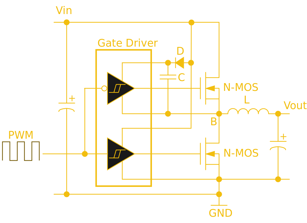
i am pretty sure the “This half-bridge power MOSFET driver circuit” has some fundamental flaws considering the inverting schmitt trigger has its negative rail connected to the output of the gate driver, but i might just be pedantic. also, for extras, i’m not sure why the non-inverting schmitt trigger has its positive rail somewhere else than the inverting one…
Weird, pretty much the only transistors I’ve lying around in my parts pile are FETs. In my opinion the current based transistors are quite awkward to use since current values cannot be easily produced in the required amount while it is trivial to generate any voltage levels. So while I am vaguely aware of how bipolar parts work but I have no intention of using them myself if I can avoid it.