If you have three hours and you want to learn the fundamentals of semiconductors, [Tiny Tapeout] has something for you: An introduction to SiliWiz. You’ll also need the SiliWiz software (or use it online), which resembles the kind of tools that chip designers use but is meant for students to use as a learning tool
Using SiliWiz, you create layers on a virtual device, and you can use Spice to view the results. The tutorial is meant to be high-level and is suggested for students aged 14 or over (but we liked it and we are quite a bit older than that). Some more advanced material is also available at the same site.
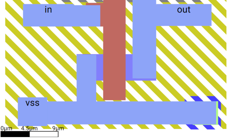
SiliWiz is easy to use. You build layers of n or p material, metal, or polysilicon. A slider lets you show a cross-section at a particular point. You label metal endpoints and use the simulation to plot the results. As expected, the process mimics a simplified version of the open-source Skywater process design kit.
We’ve had experience designing and doing failure analysis on ICs, and it is truly a different world. For example, resistors created with diffusion or polysilicon are typically difficult to make precise (that’s why you see laser-trimmed resistors on expensive precision components). However, because photolithography is very precise, the ratio of two capacitors can be a very dependable value even if the absolute value of each capacitor is less predictable. So for a digital-to-analog converter, for example, on a PCB you might use resistors, while on an IC, you are more likely to use capacitors where the ratio of values is well-known. Getting that kind of precision on a PCB with discrete capacitors would be tough.
Designing chips is not easy, and you usually want to start at a higher level and then translate your idea into silicon. SiliWiz isn’t going to give you a directly buildable design, but it will help you understand the IC design and fabrication process better.
We’ve covered the Skywater PDK before. We highly suggest you check out [Matt Venn’s] Zero to ASIC workshop if you plan to take this further.


How long till someone makes a full CPU in this?
not long. that’s why I started designing the minimalist YGREC8 core : to allow its implementation in whatever technology is available.
Build a NAND gate.
After that, it’s just a matter of scale.
How does this differ from the Magic VLSI layout tool?
http://opencircuitdesign.com/magic/
From the tutorial: “Another important tool behind the SiliWiz scenes is called Magic. It’s a powerful tool but it’s not very beginner friendly, which is one reason we wanted to make SiliWiz. Magic has been used for 40 years to help design chips! We are using it for DRC and circuit extraction.”
or the other long established software tools…
oh yeah, NIH syndrome maybe.
It’s meant as a very quick and interactive way to learn how semiconductors work – not intended to actually design something you’d tapeout.
Everything is in the browser, no downloads. Very limited set of layers to design with. And the most important factor is that it includes simulation, so you can change the transistor and see the effect immediately.
I can’t wait for EDIF imports so I can feed it my own netlist like in a PCB EDA tool :-P
> SiliWiz is easy to use. You build layers of n or p material, metal, or polysilicon.
just like any other tool at that level.
The old Carver-Mead method has not changed in 40 years :-)
Something tells me you’ve not tried drawing and simulating a mosfet using magic or the other open source freely available tools!
Honest reply : I tried Magic a year or two ago. It’s installed and it didn’t go far, I admit.
I have also used Alliance while studying at LIP6/Jussieu.
My main problem is that CS guys are not great at electronics and vice versa, so EDA tools are often really clunky, overblown, bloated, slow, with terrible UI/UX.
Oh and people persist at reinventing the wheel, such as trying to beef up Verilog with new features that have been standard in VHDL for 3 decades, and they tend to create unmaintainable millefeuille of software. You spend more time fighting the tools than actually being productive.
Pen & paper still does wonders by the way, in this context.
@Al et al (smirk)
I want to ask, perhaps, a really stupid and naïve question. Though I think it is time. Almost all the videos I’ve seen online are about doping silicon for transistors (NPN, PNP)– Can you actually also form in silicon all the other ‘basic’ components– I.E. Capacitors, Resistors, Inductors ?
I would imagine you must, but I’ve never seen a good reference on that. Or–…. Given all the external circuitry an IC needs to survive (why wouldn’t they just put it all in the chip ?).
Dumb question, I know, but this has always confused me…
AFAIK (not an expert) you can create
-diodes without any problems
-resistors but with poor precision but really good matching (look at digital to analog converters eg)
-*(really) small* capacitors
No idea for inductors, if it is possible than probably very small ones only.
Sorry, I forgot diodes– But thank you.
Inductors as well. Extra tiny but they have been done, look at RF frontends or even some attempts at onchip buck switchers of extra-close point-of-load supply (I think Intel tried it).
Also, Analog Devices implanted coils on silicon for insulated communications / digital isolators.
The general manufacturing process used in the production of chips can create quite a few different types of components. (Not just on silicon, but also for other substrate materials for that matter like GaN, SiC, GaAs, Al2O3 etc.)
The general limitations is however absolute values. An accuracy of 20% is honestly decent on an integrated circuit.
But thanks to dimensional accuracy of lithography processes it is often “easy” to get very accurate ratios between two components made with the same exposure and subsequent etching/depositioning process.
However, depositioning tends to vary in thickness over the surface of a wafer. However, features that are physically spaced close to each other tends to be more even in thickness to each other. So two resistors on the same wafer, but spaced far from each other can still be a good couple of percent different from each other.
In regards to what components can be made. More or less all of them.
Resistors are just conductors, here one can go for extra length, thin them down, or use a material that is more resistive. Adding length will however add parasitic inductance. And changing material adds manufacturing complexity. So it is debatable what is the best approach.
Inductors are just wires. And transformers are effectively just wires that have a lot of magnetic crosstalk. Take a look at a die shot of the ESP32 as an example, the transformer/balun for the WiFi section is quite obvious. But there is plenty more inductors on there, effectively the crop circles of the chip world. (but one can make them in other shapes too.)
Capacitors are just two solid metal fills separated by an insulator. But parasitic capacitance in FETs is also common way to get some “free” capacitors.
Diodes are literally just a PN junction. (P anode, N cathode) Also, diodes tends to end up everywhere in the circuit unless one builds silicon on insulators technology. (Just doping two N regions for each transistor on a P doped substrate isn’t particularly ideal if one wants an array of NPN transistors. Here one would have an N substrate and make P doped islands that one then dopes the N regions in, such that one always has a diode preventing current from flowing between one’s transistors in unintended ways.)
However, a thing to keep in mind is that some component types are hard to make “large”.
Now, logically nothing stops one from making a 1 Henry inductor on a 1 mm^2 chip, but it won’t really carry any meaningful current due to parasitic resistance, and its AC characteristics is likewise probably poor due to parasitic capacitance between the plentiful amount of “windings” necessary for such a large inductance.
We could take a quick aside into the RF world of waveguides and all the fancy stuff one can do there. But this comment is far too long already… But it is effectively the same tricks as RF wizards use on PCBs, just smaller and for higher frequencies.
In the end.
Building an integrated circuit isn’t much different than making a PCB, it is mainly just smaller.
Main difference is that on a PCB one can pick and choose semiconductors at a whim without worrying if they can be made on the same substrate or not. For integrated circuits one is generally far more limited in what combination of semiconductors one can use on a given chip.
Thanks Alexander (and others) for all the feedback,
Further, I hope my ‘stupid’ question should help those also interested in this topic. Certainly I think it is worthy of an article, or video online…. But the subject itself… Well… ‘above my paygrade’.
There is honestly very few truly stupid questions.
To be fair, a lot of more superfinal basic questions about stuff that more knowledgeable people might consider as “obvious”, are actually quite useful since a lot of severe issues tends to stem from missing obvious flaws in the most obvious places. Hybris is frankly easy to stumble into.
A great example of such an issue were heartbleed in HTTPs that were around from 2012 to 2014. That more or less allowed the client to ask for a mostly arbitrary amount of data from the webserver, a bit like a buffer overflow attack, but in reverse. So instead of overwriting server side memory, one instead gets it sent back to oneself. Often revealing tons of privet data like encryption keys and other “nice to have” stuff that the server operator really don’t want an attacker to have.
Also, to answer your original question of:
“Given all the external circuitry an IC needs to survive (why wouldn’t they just put it all in the chip ?).”
Space. All those resistors, bypass capacitors and other junk all takes space on the chip.
Bypass capacitance is often hard to get enough of on chip.
And resistors and such are often better to have externally for configurability reasons.
Anything else is often requiring specifications that is hard to integrate into the chip along with everything else one wants the chip to do. For an example, a “high” voltage power mosfet doesn’t really trivially mix with low voltage high speed logic.