
What if I told you that you might never need to draw a new footprint again? Such is my friend’s impression of the tool that she’s shown me and I’m about to show you in turn, having used this tool for a few projects, I can’t really disagree!
We all know of the JLCPCB/LCSC/EasyEDA trio, and their integration makes a lot of sense. You’re expected to design your boards in EasyEDA, order the components on LCSC, and get the boards made by JLCPCB. It’s meant to be a one-stop shop, and as you might expect, there’s tight integration between all three. If there wasn’t, you’d be tempted to step outside of the ecosystem, after all.
But like many in this community, I use KiCad, and I don’t expect to move to a different PCB design suite — especially not a cloud one. Still, I enjoy using the JLCPCB and LCSC combination in the hobby PCB market as it stands now, and despite my KiCad affinity, it appears that EasyEDA can help me after all!
All Data, No Hassle
One of the hard-to-beat EasyEDA-LCSC integration aspects is that you can easily add LCSC parts to your boards. There’s no need to hunt for footprints and symbols, they’re all ready to go. You simply get the LCSC inventory at your fingertips, or at least the part of it that’s been documented by EasyEDA engineers. Indeed, this information isn’t just EasyEDA-specific, you can access it externally, and there’s a tool called easyeda2kicad that lets you download all the part files in KiCad format!
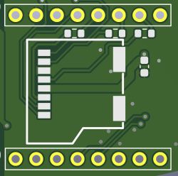
For instance, I was recently looking for microSD sockets — something that I have a tried and true part for. There’s a few hundred pieces in a bag next to my desk, even. Today’s constraint? It has to be less wide than the card itself, since I have to fit it into a narrow spot. Mouser didn’t have any good parts for me, but LCSC did. The sockets I found were also way cheaper, even including shipping and VAT. So, I’ve found a good part, but oh no, the footprint has ten pads and the mechanical dimensions are only half-intelligible, and I just want to get to drawing the long overdue board already!
All you need from here is the easyeda2kicad script installed – it takes the LCSC part number and creates the symbol, footprint and 3D model files for you automatically. To be clear, not all LCSC parts have been digitized. But that said, for one project of hers, my friend could successfully download a whole MXM slot, DisplayPort, miniDisplayPort and VGA connectors, and a few inductors with non-standard footprints; a combination that would typically need you to sit down in front of a PCB editor for a few hours, and that’s certainly not including the 3D models.
Limited, But Great Nevertheless
Choice in EDA software is something way less malleable than component and PCB service choice, and it rocks that this software now gives us an extra option. I’ve gone through a few projects by now with this script at the ready, the footprints and symbols have all worked as advertised, and while I still need to design footprints every now and then, they’re usually something exotic.
easyeda2kicad will absolutely help if, like me, you have a foot strongly in the JLCPCB+LCSC field. Or the Eastern parts field at all. I’ve given a good few thousand dollars to these two companies, for personal and business purposes alike, and I don’t see a reason I’d stop just yet. I’m not here to promote any specific company, of course, and you’ll guess correctly that I’ve had these footprints and symbols work for Aliexpress parts, too, as long as you find which LCSC part they correspond to.
There are, of course, a few problems. The footprints have dubious legal status — any license granted likely doesn’t include such external use, and while we wouldn’t foresee problems adding such parts to open-source projects, it’s a technicality to keep in mind. These symbols and footprints are untested unless we know otherwise, unlike parts in the KiCad library, and as usual, they might deviate from datasheet in important ways.
You’re also at the mercy of the EasyEDA API, which you might remember [Jan Mrazek]’s irreplaceable LCSC search tool had problems with in the past. The problems have since been resolved, but the situation has left a bad aftertaste.
You might think that this is free symbol and footprint galore, and in a way, it is! Of course, the LCSC-JLCPCB-EasyEDA trio still wins — you’re more likely to use their services if you use this tool. There’s a reason why Western manufacturers often provide the same services, giving you footprints, symbols and 3D models so that you have it easier starting a new design within their ecosystem. SnapEDA, a similar service for Western parts, has been a mainstay in the electronics world, and to think of it, it’s long overdue to have such an option for Eastern parts!


“Never X Y again!” is clickbait since before Internet was even a thing.
Interpret it as “greatly reduce, up to 100% in many cases”, and you’ll be set. Reducing occurrence of something to zero in all instances is seriously rare given just how multifaceted our world is. On the other hand, I do have to stay that I no longer draw footprints from datasheet dimensions, and I do a fair bit of work.
He’s saying it’s a tell. A linguistic sign that what’s to follow is an advertisement.
If writing non ads, it might be better to avoid this language.
Besides libraries of component footprints are nothing new.
If this one is ‘complete’, it’s only for a moment in time, same as the others were.
Efforts are always made…Heat death of the universe, therefor hookers and blow!
This library’s neither new nor complete, but it doesn’t claim to be – it’s a valuable addition to a hacker’s arsenal, and stands out due to covering Eastern parts as we have them now. Hell yeah I’ll use ad language to “sell” this tool to people – why would I write this article if I didn’t think this tool were valuable enough to “sell” in such a way?
To give a fair assessment of the strengths and weaknesses of one of many competing solutions to a common problem?
I know crazy talk.
I’ll just leave this here:
https://www.youtube.com/watch?v=9h9wStdPkQY
that’s what I’m doing in the article, have you read it? a fair assessment of the strengths and the weaknesses. summary: it’s an awesome tool.
Make up your mind, is it an ad or a fair assessment?
Can’t be both.
If it truly is a fair assessment, you might want to avoid language that puts you in a group you should want to avoid.
It can absolutely be both an ad and a fair assessment, that’s exactly what I’m doing 😎
Yes, indeed.
I nearly disregarded the whole article for that.
Good tools for schematic symbols and PCB footprints are an absolute must in a good PCB package (and KiCad’s are quite good). There will always be footprints which are not in any database. I have designed several footpints for home-brew adapters that are not available in any shop. No need even trying to find such a thing on the ‘net.
But apart from that. Being able to find and integrate footprints from other sources is a nice thing to have. I guess this is just an alternative for Samacsys, PCB Libraries, Ultralibrarian, SnapEDA, and a bunch of other sources.
And even so, it’s quite possible you end up modifying such footprints to fit your needs anyway. An example was a project where I had to put two RJ45 connectors next to each other. I deleted one of the holes from one connector, to fit the metal shielding of both connectors into the same hole.
So again, Good tools are a must, external libraries can save (but also waste!) time.
SnapEDA is no decent alternative, it used to work with KiCAD 5, but since then it has not been updated, and the only thing they propose is a clunky M$ app. Mac and Linux users are left alone.
This is very exciting. It’s been a while since I’ve had a PCB made, mostly due to time limitations. I’m not looking to make anything particularly demanding from an EE perspective, and I’m not looking to order anything but maybe one or two ICs from a vendor outside of the tightly coupled LCSC catalog and JLCPCB assembly service.
I’ve found that, with this set of requirements, the biggest time sink by far is pulling in footprints/symbols for things that aren’t in the base KiCAD catalog. Running a script, slapping a symbol down, and routing sounds much nicer than faffing around for 30+ minutes every time I want to pull in a buck converter or flash memory chip.
Until you get the boards back and put the part on a footprint that’s just obviously wrong. At which point you bang your head against the top of the table, and swear never to blindly trust things again. (Before you do it again in a few years, obviously).
Buck converters are usually the common culprits too, since they very frequently have non-standard footprints, and a lot of the “here’s your footprint!” tools rely on recognizing the package name. Or they generate some of the weird copper pad geometries in different ways and so depending on the tool, they might get imported entirely wrong.
I wish they all had better ways of indicating “yes, this has been confirmed to work when imported into this specific EDA.”
That’s never a guarantee, especially with drawing things yourself – however, this tool often provides 3D models, so statistically, you’re better off than with your own design! Either way, if you don’t print your board out and verify, you’re relying on some amount of luck, whether your footprints are self-drawn or borrowed. When it comes to copper geometries, I’ve been there with SnapEDA, but it’s not been a problem so far with easyeda2kicad. As for recognizing the package name, I try to do that too when I look through datasheets 😅 at least with EasyEDA, there’s a chance of external intervention, that is, if I even run easyeda2kicad in such a case and don’t just decide to use a stdlib footprint I falsely recognized!
Yeah, but it’s more the “running a script, slapping a symbol down, and routing” mindset that’s dangerous. Printing a board out before routing’s a great way to check. For expensive multilayer boards I also usually produce an unrouted 2 layer board first to check footprints (and physical dimensions) – they’re so cheap and fast that it’s totally worth it. I don’t think I’ve ever done it without realizing something could be done better, so it’s always paid for itself easy.
The assembly house I frequently use actually wants to check package dimensions against a footprint before assembly, and so the recent trend of manufacturers providing footprints (via SnapEDA/UltraLibrarian/etc.) rather than actual dimensions causes problems.
“redrawing things yourself, slapping them down, and routing” is alike dangerous, even if for other reasons. Lack of crosschecking will get ya. I can assure you that “running a script” saves you some pretty valuable time you could spend checking the new footprint’s validity. The unrouted 2 layer practice is good, but, it won’t gain much hold as it’s a time&money investment – in the end, relying on someone else’s tested footprint is pretty good, and EasyEDA footprints are a reasonably close match, even if a bit of black box wrt their origins. Also, “footprints rather than dimensions” does sound troubling, wouldn’t touch that with a long stick, who even does that? got names?
I think it’s Analog Devices, actually. It’s on newer chips, since obviously older ones have it in datasheet.
Yup, it’s Analog. On newer parts they only have dimensional drawings for the package itself, not the footprint. Footprints are only available through UltraLibrarian and SamacSys.
In the words of Ronald Reagan, Trust but Verify.
Having been an Eagle guy for around 30 years and more recently a KiCAD believer, I’ve had my share of bad footprints. I always print a 1-1 PCB on paper and dry fit my components. That pretty much avoids the problem. OK, never 100% but definitely catches the brain-f@rts.
I was going to ask why people aren’t test printing their PCBs. It’s been a while since I’ve designed a board, but I was taught to design PCBs on computer and always do a test print to check component footprint, size, orientation, etc.
I wasn’t taught to do this, but after a few preventable mistakes I learned it all by myself :-)
I print the component side of my PCB on plain old A4 paper, then lay any tricky SmDs on top to make sure they look right. Through-hole components get poked through the paper to check that all the pins and mechanicals line up with the footprint.
It’s not perfect but you can also use your printed paper PCB to make sure you haven’t made outrageous mistakes with the enclosure, panel cutouts etc. It won’t guarantee 1 um precision on your cutouts but it will let you know if the “centre” of a cutout has somehow moved to the “corner” or if you’ve forgotten to allow for the thickness of the PCB itself…
Oh don’t worry, I like reading datasheets, and will happily spend the 2 minutes cross referencing the symbol to the pinout. For the footprint and routing, though, JLCPCB will do a continuity test for a small upcharge. Incorrect geometries (wrong pin pitch, etc) will get caught.
If something does slip through, then either it’s me, the script or the source data. If it’s me or the script, any board I get made isn’t too expensive, and I’ve experienced worse delays for more mundane reasons. If it’s the source data, I find board shops will rectify their mistakes (again, with those mundane delays).
yeah, I check my symbols&footprints whenever there’s a visible mismatch, especially given that quite a few parts (i.e. CH334) come in “one package, many pinouts” flavor. would like to know more about the JLCPCB option – never seen such a thing, and I do order there from time to time!
So much this.
If you are paid to do this work for a living, and this happens, it’s… not a good look. “Didn’t you check?”
Also, IPC class compliant footprints are what I design and use to ensure the design can be consistently made.
It’s annoying to design footprints, however, once done and reviewed, you don’t have to do it again. This could be said for functional subcircuits.
Altium’s snippets carry the library concept forward to design blocks. I wish it had a better tagging system, but its certainly helpful.
This is exactly how easyeda2kicad workflow goes! So, yep, look into it and let us know how it goes for you^^
SamacSys’ “Library Loader” is pretty handy for pulling in parts to KiCAD. A lot of time I go to Digikey or Mouser and they’ve got models to download, then the Loader picks them up in my download directory and auto-populates them in KiCAD. Pretty sweet, although the symbols tend to be just boxes with pins hanging from them so not as cool or informative to look at. Sometimes I go back and touch them up with a cut-n-paste from an existing symbol for stuff like FETs, diodes, whatever.
Yeah, I’ve used it some, and it works well enough. That’s what I’ve used in the past for projects where I’ve ordered my BoM and soldered it up myself. It takes a little more time than running a python script, though, and I seem to recall some clunkyness around the software (it’s been a couple years now).
Fact of the matter is, though, for any board I’m ordering nowadays I’m willing to spend a good chunk of change to get it assembled (except for maybe an MCU or FPGA that LCSC doesn’t stock), I simply don’t want to spend the time to inventory and solder up 50+ componenents. The library loader theoreticall works for PCBway and asking them to order through Digikey or Mouser, but last time I gave them a BoM and asked them to order through Mouser it was a nightmare of delays. Took me 2 months of timezone-constrained emails to get my boards.
I’ll almost definitely be trying JLCPCB, LCSC, and this script next time.
Since a footprint of a component varies on your design requirements and the process used to build your board you will never be able to just plop a pre defined footprint and get good results. When I designed boards I had to adjust footprints constantly to minimize rework and maximize circuit performance. What worked great for one project wasn’t always acceptable for another even using the same build house.
What you’re talking about is not relevant here – KiCad lets you adjust footprints per-part, no matter if they’re stock, imported or self-drawn, and I do that constantly too. Using easyeda2kicad is about quickly getting a base footprint with a degree of verified-ness to it, not about never adjusting your footprints according to the situation.
Getting “PydanticUserError: The `field` and `config` parameters are not available in Pydantic V2, please use the `info` parameter instead.” using Python 3.11.4 on Windows. Am I doing something wrong?
Pydantic is a bit pedantic (ha!) about its API version. The workaround is to downgrade the version:
https://github.com/uPesy/easyeda2kicad.py/issues/94
Works now, thanks!
Bummer, doesn’t run on my machine, I’ve filed an issue report on github.
One thing that I’ve found with an unreasonably large number of JLCPCB components (switches, sd card connector, usb connectors) is that while the datasheet has a fairly thorough mechanical layout and footprint, they don’t define the actual center of the component. grrr. How ya gonna get that placed correctly??? I have a micro SD card connector that I have never quite gotten the center correct. Fortunately the JLCPCB techs fix it (I leave copious notes about that) but would rather not have to depend on some overworked tech to make it right.
It’s normal for SMD technicians to correct placements manually, especially for components where the centre isn’t easy to define.
Pick and place machines tend to define their own component centres based on the images they get of the component bottom and whichever model they’re using for that component. I had a run of SBCs before with a DIMM slot on them, and the pick and place defined the placement coordinate on that type of component as the middle of the pad for pin 1, at one end of the slot. This was confusing until I realised this was a convenient place for the machine vision to find on the component, and for the technician to manually teach on a PCB.
The pickup coordinate obviously has to be closer to the centre, but this only gets used insofar as to get a component from the feeder and stuck to the nozzle, and is basically discarded once the component camera has a look.
Also I’d wager that JLC have a tried and tested internal database of placement centres for the components they offer, which gets used automatically when you stay within their ecosystem.
This website has worked well for me. Download the EasyEDA project file and upload and it downloads a KiCad footprint. https://wokwi.com/tools/easyeda2kicad
This is rather timely. Just the other day I watched a video where something was designed in EasyEDA, and the ease of importing footprints impressed me. I’ve been debating designing a board myself, but I’d rather use KiCad. This tool is the missing link. I’ll definitely have to play with it.
I don’t use kicad, since I live in the Eagle / Fusion360 world. For me, SnapEDA / Samacsys Library loader has worked 90%, but usually there is some small “gotcha” stuff that needs anyway fixing, like thermal pad vias or need to add some keepaway / restrict layers to prevent routing or copper pours too near. But mostly I like that very often the 3D footprints are included.
If that script would work….
Again, something written in python that simply does not work.
Installed it, and just got the mess below.
When will people start going away from that shit python is!
Traceback (most recent call last):
File “.local/bin/easyeda2kicad”, line 5, in
from easyeda2kicad.__main__ import main
File “.local/pipx/venvs/easyeda2kicad/lib/python3.11/site-packages/easyeda2kicad/__main__.py”, line 12, in
from easyeda2kicad.easyeda.easyeda_importer import (
File “.local/pipx/venvs/easyeda2kicad/lib/python3.11/site-packages/easyeda2kicad/easyeda/easyeda_importer.py”, line 6, in
from easyeda2kicad.easyeda.parameters_easyeda import *
File “.local/pipx/venvs/easyeda2kicad/lib/python3.11/site-packages/easyeda2kicad/easyeda/parameters_easyeda.py”, line 26, in
class EeSymbolPinSettings(BaseModel):
File “.local/pipx/venvs/easyeda2kicad/lib/python3.11/site-packages/pydantic/_internal/_model_construction.py”, line 130, in __new__
cls.__pydantic_decorators__ = DecoratorInfos.build(cls)
^^^^^^^^^^^^^^^^^^^^^^^^^
File “.local/pipx/venvs/easyeda2kicad/lib/python3.11/site-packages/pydantic/_internal/_decorators.py”, line 441, in build
res.validators[var_name] = Decorator.build(
^^^^^^^^^^^^^^^^
File “.local/pipx/venvs/easyeda2kicad/lib/python3.11/site-packages/pydantic/_internal/_decorators.py”, line 249, in build
func = shim(func)
^^^^^^^^^^
File “.local/pipx/venvs/easyeda2kicad/lib/python3.11/site-packages/pydantic/_internal/_decorators_v1.py”, line 77, in make_generic_v1_field_validator
raise PydanticUserError(
pydantic.errors.PydanticUserError: The `field` and `config` parameters are not available in Pydantic V2, please use the `info` parameter instead.
For further information visit https://errors.pydantic.dev/2.1.1/u/validator-field-config-info
A little less time complaining about Python, a little more time reading – a few comments above you someone had the exact same problem and someone else found the solution!