A common joke in electronics is that every piece of wire and PCB trace is an antenna, with the only difference being whether this was intentional or not. In practical terms, low-frequency wiring is generally considered to be ‘safe’, while higher frequency circuits require special considerations, including impedance (Z) matching. Where the cut-off is between these two types of circuits is not entirely clear, however, with various rules-of-thumb in existence, as [Sebastian] over at Baltic Lab explains.
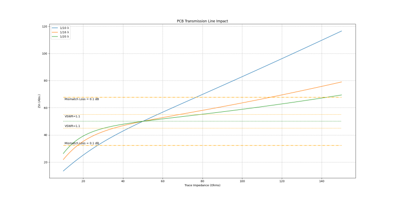
A popular rule is that no impedance matching between the trace and load is necessary if the critical length of a PCB trace (lcrit) is 1/10th of the wavelength (λ). Yet is this rule of thumb correct? Running through a number of calculations it’s obvious that the only case where the length of the PCB trace doesn’t matter is when trace and load impedance are matched.
According to these calculations, the 1/10 rule is not a great pick if your target is a mismatch loss of less than 0.1 dB, with 1/16 being a better rule. Making traces wider on the PCB can be advisable here, but ultimately you have to know what is best for your design, as each project has its own requirements. Even when the calculations look good, that’s no excuse to skip the measurement on the physical board, especially with how variable the dielectric constant of FR4 PCB material can be between different manufacturers and batches.
Heading image: Input impedance plotted as a function of trace impedance for trace lengths of 1/10, 1/16, and 1/20 of a wavelength. (Credit: Baltic Labs)


Good to see, trend to higher frequencies on the march though dimensions smaller too. Guidelines helpful, thanks for posting and nice level of diversity on this forum too, well done :-)
I would venture so far as to say that if you want to minimize emissions that the trace length should be a non-integer multiple of the frequency of interest (and its harmonics).
Ah, my understanding is a 1/4 wave long antenna is fairly efficient ie the so called whip.
So then a rather shorter distance than 1/4 of equivalent wavelength for the frequency of interest
would be a target.
Also where the equivalent frequency of the signal rise time translated to 1/4 wavelength too
influenced more so I’d expect by the drive current capacity into a comparatively heavy capacitive load…
So if your design fits inside 10cm x 10cm (a common limit for cheap PCBs), and your components are worst case (diagonal corners, about 14 cm) your wavelength is 16x14cm = 2.24 metres. Which makes maximum clock about 134MHz.
So – if you limit your clock to 120MHz, or have your main chip in the middle of your board for designs up to about 230MHz, you should be OK. Larger designs, of course, need more caution.
What your calculations fail to take into account are rising/falling edges of those clock pulses. 120MHz (or 230MHz) is only the fundamental frequency – there’s an infinite sum of odd harmonics in a square wave so a 120MHz clock also has a 360MHz component, a 600MHz component, etc. Granted, those components are less in magnitude as they increase in frequency, but they’re still present and they’ll still radiate.
You’d need to limit your maximum *rise time bandwidth* to ~230 MHz. So any digital line with an edge faster than 2ns will start to cause trouble. It’s all to easy for a slow clock to drive it’s output far harder than needed. Nice clean square waves look pretty, right until you being them into the EMC chamber.
Yeah, this isn’t actually really a question of trace impedance, it’s a question of termination. Even a slow clock being splayed all over a board can cause problems if it’s improperly terminated – and even a fast clock on a super-tiny trace will generally be fine if it’s terminated well.
Roughly one foot per nanosecond. So technically it doesn’t matter when what you’re looking at can get to you in less time than your sensor needs to determine the transition period of the signal.
Don’t forget the skin effect. Designing some things with polarization in mind, trace width and trace thickness can carry different signals at the same time.
A foot per nanosecond only in free space. On a PCB it’s substantially less. In buried traces (stripline) it’s half(-ish, depending on material).
Trace width is something that is easily controlled. I like to use atlc2 to guesstimate the proper geometry, including via fencing to get a well-defined impedance.
It’s also possible to get 50 Ohm on 1.5mm FR4, but then the track is rather wide.
At higher frequencies, I tend to worry more about changing planes and the use of via barrels in general. These invariably introduce an impedance discontinuity, and it’s not immediately obvious how much of an impact they have.
Very high speed designs seems to favor back drilled vias to remove the ~1mm stubs – talking about being paranoid. But for most purposes including basic ethernet and USB (not Superspeed), worrying about vias is probably a bit too much.
“It’s also possible to get 50 Ohm on 1.5mm FR4, but then the track is rather wide.”
You just need to use a ground-backed coplanar waveguide structure.
The key for impedance matching is basically the distance from the trace to its return current (inductance) relative to its overall dimension (capacitance). With, say, a 2-layer 1.5 mm FR4 with signal on top and ground on bottom, it’s got a 1.5 mm distance to ground. In that case you need nearly 2.9 mm trace width.
So you need to reduce it. Bring the ground to the top layer, right beside the signal. You can get 0.1 mm track-to-track spacing on PCBs cheaply now, and when you do that, obviously the trace width needed drops dramatically.
Even with the adjacent grounds, overall it’s still smaller! About 0.2 mm width, 0.1 mm gap (x2), and even 1 mm ground width (x2) is less than the 2.9 mm width needed, and that ground width is overkill.
“These invariably introduce an impedance discontinuity”
You can design a transmission-line structure using vias between top and bottom that matches your impedance target. You’ll still get a bit of a mismatch because the transmission modes are different, but it’s not bad. In fact, if you use a coaxial calculator and just put 4 vias at that spacing around the signal (and clear out the interior) it’s extremely close.
Sounds like you remember Grace Hopper’s Rule: a nanosecond a foot. Memorialised with 1 foot long pieces of telephone wire she used to hand out.
Coax, actually… had a piece (yellow) she handed my father during a lecture, but I forgot what it was a number of years back and threw it away while cleaning out my junk drawers. It wasn’t until months later my memory was jogged and regretted being so hasty in my cleanup. Whatcha gonna do…
Yellow coax was most likely a length of the original Ethernet cabling. It was pretty large diameter with a solid core center as “drops” were vampire tapped with a drill. Yellow was the default color for Ethernet coax. Light blue was for Dec’s CI (computer interconnect) connections.
Aaaugh: the “1/10th rule” isn’t *trace length*, it’s distance from *source* to *load*. If your “source” is off-board – like, say, a connector – you better match it as well as you can, because your effective distance can be huge.
It’s interesting that the top picture is of a SAW filter. SAW filters are *notoriously* sensitive to mismatch, and their broadband performance can be affected by surprisingly minute shifts in terminating impedance. It would be interesting to see an S21 plot of that board with both ideal and nonideal trace impedances. I wouldn’t be surprised to see 60dB of rejection suddenly drop to 40dB, or surprise resonant peaks suddenly appear.
Interesting that the subject of the experiment was a SAW filter. SAW filters are *notoriously* sensitive to broadband input and output termination impedance. It would be interesting to see an S21 plot of this board with both ideal and nonideal transmission line impedances. I wouldn’t be surprised to see 60dB rejection suddenly drop to 40dB somewhere, or surprise resonances in the stopband suddenly appear.
A few remarks:
1) the criterion here is mismatch loss, targeted below 0.1 dB. That may be fine for analog design, but for digital, you are more interested in the integrity of the signal than in minute variations on its amplitude.
2) Someone remarked that the SAW filter is no coincidence. I agree: mismatch, I particular of out-of-band frequencies leads to reflections, possibly even standing waves, and an increased radiated coupling between input and output, limiting stopband rejection.
Anyone remember ECL?
Emitter Coupled Logic circuits were a pain; trace length, curvature and cross-section were all critical factors.
No sharp corners, smooth curves only.
Ah, this has me starting to recall the “arguments” we students would “carry” back and forth, between our EMC and embedded systems professors, when I was in engineering college.
In digital designs, echos from signals with rapid transitions can cause problems like false triggers on flip-flop inputs, or missed triggers. I’ve seen effective clock rates doubled or halved, depending upon the particular conditions. Plan for a large safety margin or you’ll see problems in production.