Input impedance plottet as a function of trace impedance for trace lengths of 1/10, 1/16 and 1/20 of a wavelength. (Credit: Baltic Labs)

When Does Impedance Matching A PCB Trace Become Unavoidable?

A common joke in electronics is that every piece of wire and PCB trace is an antenna, with the only difference being whether this was intentional or not. In practical terms, low-frequency wiring is generally considered to be ‘safe’, while higher frequency circuits require special considerations, including impedance (Z) matching.  Where the cut-off is between these two types of circuits is not entirely clear, however, with various rules-of-thumb in existence, as [Sebastian] over at Baltic Lab explains.

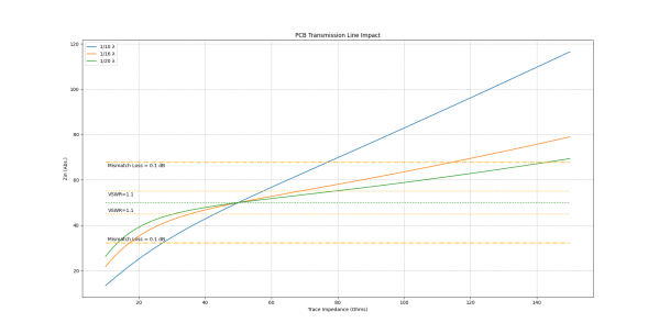
A popular rule is that no impedance matching between the trace and load is necessary if the critical length of a PCB trace (lcrit) is 1/10th of the wavelength (λ). Yet is this rule of thumb correct? Running through a number of calculations it’s obvious that the only case where the length of the PCB trace doesn’t matter is when trace and load impedance are matched.

According to these calculations, the 1/10 rule is not a great pick if your target is a mismatch loss of less than 0.1 dB, with 1/16 being a better rule. Making traces wider on the PCB can be advisable here, but ultimately you have to know what is best for your design, as each project has its own requirements. Even when the calculations look good, that’s no excuse to skip the measurement on the physical board, especially with how variable the dielectric constant of FR4 PCB material can be between different manufacturers and batches.

Heading image: Input impedance plotted as a function of trace impedance for trace lengths of 1/10, 1/16, and 1/20 of a wavelength. (Credit: Baltic Labs)

Continue reading “When Does Impedance Matching A PCB Trace Become Unavoidable?”

Wires Vs Words — PCB Routing In Python

Preferring to spend hours typing code instead of graphically pushing traces around in a PCB layout tool, [James Bowman] over at ExCamera Labs has developed CuFlow, a method for routing PCBs in Python. Whether or not you’re on-board with the concept, you have to admit the results look pretty good.

GD3X Dazzler PCB routed using CuFlow

Key to this project is a concept [James] calls rivers — the Dazzler board shown above contains only eight of them. Connections get to their destination by taking one or more of these rivers which can be split, joined, and merged along the way as needed in a very Pythonic manner. River navigation is performed using Turtle graphics-like commands such as left(90) and the appropriately named shimmy(d)that aligns two displaced rivers. He also makes extensive use of pin / gate swapping to make the routing smoother, and there’s a nifty shuffler feature which arbitrarily reorders signals in a crossbar manner. Routing to complex packages, like the BGA shown, is made easier by embedding signal escapes for each part’s library definition.

We completely agree with [James]’s frustration with so many schematics these days being nothing more than a visual net lists, not representing the logical flow and function of the design at all. However, CuFlow further obfuscates the interconnections by burying them deep inside the wire connection details. Perhaps, if CuFlow were melded with something like the SKiDL Python schematic description language, the concept would gain more traction?

That said, we like the concept and routing methodologies he has implemented in CuFlow. Check it out yourself by visiting the GitHub repository, where he writes in more detail about his motivation and various techniques. You may remember [James] two of his embedded systems development tools that we covered back in 2018 — the SPI Driver and the I2C driver.