A few years back NVIDIA created a dedicated cryptocurrency mining GPU, the CMP 170HX. This was a heavily restricted version of its flagship A100 datacenter accelerator, using the same GA100 chip. It was intended for accelerating Ethash, the Etherium proof-of-work algorithm, and nothing else. [niconiconi] bought one to use for accelerating PCB electromagnetic simulations and put a lot of effort into repairing the card, converting it to water-cooling, and figuring out how best to use this nobbled GPU.
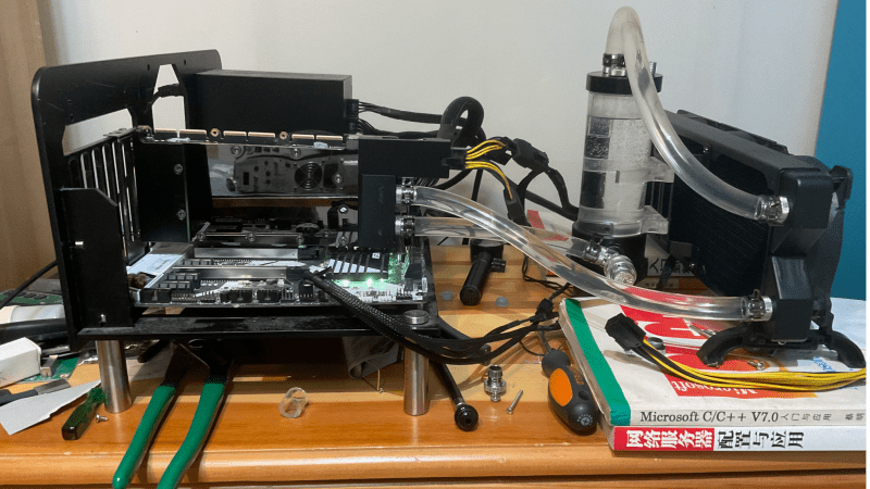
Typically, the GA100 silicon sits in the center of the mighty A100 GPU card and would be found in a server rack, cooled by forced air. This was not an option at home, so an off-the-shelf water-cooling block was wedged in. During this process, [niconconi] found that the board wouldn’t power on, so they went on a deep dive into the power supply tree with the help of a leaked A100 schematic. The repair and modifications can be found in the appendix, right down to the end of the article. It is a long read to get there.
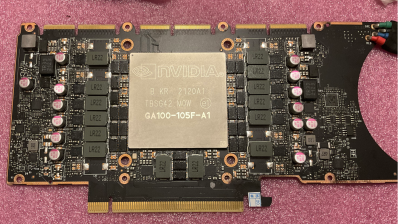
NVIDIA has a history of deliberately restricting silicon in consumers’ hands to justify the hefty price tags of its offerings to big businesses, and this board is no different. The plan was to restrict the peak performance of the board to only applications with the same compute requirements as Ethash, specifically memory-intensive algorithms. The FP64 performance was severely limited, but instructions were not removed. This meant the code would run really badly, considering what the GPU is capable of.
The memory was limited to 8 GB, despite some A100 cards hosting a whopping 80 GB. The strategy was to use fuses to limit the crucial instructions, particularly the FP32 FMA and MAD instructions, which are used for multiply-add operations and are crucial for general computing applications. Finally, the PCIe bus was nobbled to run only as a Gen 1 interface with a single lane. They reduced the lane count by removing the coupling capacitors on the PCB, which meant they could just be added later, but it’s still only a slow interface.
[niconconi] went into great detail benchmarking the instruction types, keeping their EM simulation application in mind. After a few tweaks to make it work, they determined it was a good purchase. This article is worth reading for all those hardcore GPU nerds!
If you need a primer on GPU mining, we’ve got you covered. Once you’ve understood proof-of-work crypto, perhaps take a look at Chia?
Thanks to [gnif] for the tip!


I’m looking into buying an nVIDIA Tesla M40 24GB for running LLMs. They seem to be cheap enough these days but I still cannot say any GPU with LLM worthy VRAM is a good deal
The article’s conclusion is a little misleading. [niconconi]’s main conclusion really is: “Overall, this GPU is mostly useless. It can still be useful only when your have a specific niche”
He also concludes that it was a good purchase – for him – because despite the heavy limitations, his very specific need for FDTD electromagnetic field simulations was still fitting into the limitations and getting huge acceleration.
Yeah the actual recommendation that was relevant a year ago, was buy those chinesium MI50 hybrid cards used for mining
At this stage it’s just better to transplant the gpu die onto a custom pcb. Already being done in China
Not so helpful if the fuses in the chip haven blown to nobble the performance. Unless of course the fuses aren’t really fuses at all and can be reprogrammed with some stolen software. For some chips I worked on there where OTP ROM IPs which were blown at production test. No way to undo that. On others we used bond option programming, so it was fixed inside the package. I imagine the Chinese would still find a way around even that, if there was profit to be made!
yea just, its only a couple pins and a hair dryer right?
anyone had success installing a CMP 170HX in Ubuntu server 20.04 ? can’t sem to get card recognized at boot and drivers and tools will not load – set BIOS to CSM disabled, virtualization disabled,