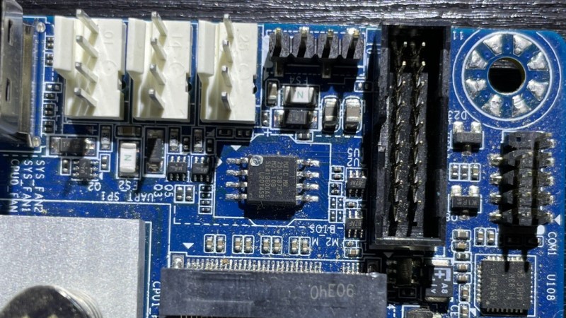
Some hackers have the skills to help us find noteworthy lessons in even the most basic of repairs. For instance, is your computer failing to boot? Guess what, it could just be a flash chip that’s to blame — and, there’s more you should know about such a failure mode. [Manawyrm] and [tSYS] over at the Kittenlabs blog show us a server motherboard fix involving a SPI flash chip replacement, and tell us every single detail we should know if we ever encounter such a case.
They got some Gigabyte MJ11-EC1 boards for cheap, and indeed, one of the BIOS chips simply failed — they show you how to figure that one out. Lesson one: after flashing a SPI chip, remember to read back the image and compare it to the one you just flashed into it! Now, you might be tempted to take any flash chip as a replacement, after all, many are command-compatible. Indeed, the duo crew harvested a SPI chip from an ESP32 board, the size matched, and surely, that’d suffice.
That’s another factor you should watch out for. Lesson two is to compare the SPI flash commands being used on the two chips you’re working with. In this case, the motherboard would read the BIOS alright and boot just fine, but wasn’t able to save the BIOS settings. Nothing you couldn’t fix by buying the exact chip needed and waiting for it to arrive, of course! SPI flash command sets are fun and worth learning about — after all, they could be the key to hacking your “smart” kettle. Need a 1.8 V level shifter while flashing? Remember, some resistors and a NPN transistor is more than enough.


BIOS engineer here. There are SPI commands to ID the ROM chip. Some BIOS’s have a table that tell the BIOS how to use each supported chip. If the chip isn’t found in the table, functions that use the table, like the functions to write to the ROM, will throw an error.
I´ll chyme in:
depending on this ID there are also different timings applicable for a given chip. So even if you´d man-in-the-middle fake those IDs you might still stumble on the timings used.
One could think that a SPI flash chip command set would be simple enough not to need 15 different standards.
It is the extensions that kill. Each vendor will extend the standard with some nifty stuff that could be very useful…
Everything to do with single line reads and writes are well-standardized, but that’s not fast enough for people, so there are also 2-line I/O and 4-line I/O, plus wiher-than-24-bit addresses, and all the different ways people implement more than one status register (which some manufacturers then also split into a separate configuration register, or multiple commands for different bytes of the status register). And don’t forget extended features like secured OTP, password protection, block locking, etc. Even the erase size may be different between parts. If all you want to do is read the flash with one I/O line, that’s well-known. The moment you try to do anything else, you have to read the datasheet to be sure. SFDP helps, but I rarely see it implemented on the host. Most devices are programmed specifically for the part chosen.
“Everything to do with single line reads and writes are well-standardized”
They are by now, because the earlier disaster is mostly past: 03h will work for most reasonable-ish frequencies. But go back and look up the early Atmel DataFlash series – you won’t see 03h or 0Bh commands at all there, because you needed E8h for a continuous data read. And the point at which you needed to swap between 03h/0Bh was random for a while. This is why older FPGAs literally had pins which chose which SPI command they used at boot to start reading.
Thankfully I’m pretty sure those early ones are now far gone, and the DataFlash compatible ones still in existence also implement 03h/0Bh.
The dead bits is my worry with TPM. I have no hate for TPM, but many BIOS write to slow SPI to store data (which I know for a fact because a bug that caused hanging in Windows was fixed, it detailed the slow SPI writes).
Now back on track: If there is a continuos write lope, even so every 10 minutes, I can see why NOR SPI flash would die faster these days. With only 100k cycles I can see it happen shortly outside of warranty, if a consumer system is on 24/7. Honestly whatever checks Windows runs against fTPM in operation, we have non-volatile FeRAM for such tripes.
The standard TPM2 model is to store private keys on disk, encrypted by a storage key on the TPM so only the TPM can decrypt and use them. After initialization TPM2 rarely stores anything to flash. If I remember correctly, one of the approaches is to literally set up a storage root key and a few other bits and then set and forget a random password for the Owner auth so nothing can tamper with TPM flash without going through the BIOS menu and wiping the whole thing using Platform auth.
Of course, I guess all bets are off for a firmware TPM that also shares flash with the EFI variables. Maybe just another reason physical TPM is better if you aren’t MS and actually use the parameter encryption and other security features.
Wouldn’t encrypted keys on the disk be designated by the operating system and/or disk encryption driver?
Also, it isn’t quite that simple for the TPM to decrypt this, as during boot integrity checks are collected for the firmware, critical firmware settings (like Secure Boot status, boot order, etc.), and the bootloader before the TPM can release the key.
@Steven Clark, in my defense:
“The document states that AMD has found that certain AMD Ryzen™ system configurations intermittently perform extended fTPM-related memory transactions in SPI flash memory (“SPIROM”) on the motherboard. This can cause temporary pauses in system interactivity or responsiveness until the transaction completes.”
Obligatory xkcd https://xkcd.com/927
The only way we’ll probably see true universal standards is when we invent time travel. When a competing standard is created all the benefits are added as a patch to the current standard. Then you send a T100 back in time to deliver the patch and stop the competing standard from being created.
I just used hot air to take my chip off and write it. It was a Macronix 73F chip. But oddly enough the Intel FIT tool Identified it as a 73E.
My chip is not broken as far as I know, I just wanted to use a B250 motherboard with a modified BGA1440 8-core CPU. Which involves injecting new microcode and Intel ME with the ‘CoffeeTime’ utility.