Anyone who’s spent significant amounts of time salvaging old electronics has probably wished there were a way to take apart a circuit board without desoldering it. [Zeyu Yan] et al seem to have had the same thought, and designed circuit boards that can be dissolved and recycled when they become obsolete. Read the details in the research paper. (PDF)
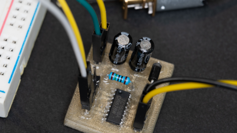
The researchers printed the circuit boards out of water-soluble PVA, with hollow channels in place of interconnects. After printing the boards, they injected a eutectic gallium-indium liquid metal alloy into these channels, populated the boards with components, making sure that their leads were in contact with the liquid alloy, and finally closed off the channels with PVA glue, which also held the components in place. When the board is ready to recycle, they simply dissolve the board and glue in water. The electric components tend to separate easily from the liquid alloy, and both can be recovered and reused. Even the PVA can be reused: the researchers evaporated the solution left after dissolving a board, broke up the remaining PVA, and extruded it as new filament.
The researchers designed a FreeCAD plugin to turn single or multi-layer KiCad circuit layouts into printable files. They had to design a few special sockets to hold components in place, since no solder will be fastening them, but it does support both SMD and through-hole components. The traces have a bit more cross-sectional area than normal copper traces, which has the advantage of compensating for the liquid alloy’s higher resistance; their standard traces had no trouble dissipating heat when carrying 5 amps of current. As a proof of concept, they were able to make a Bluetooth speaker, an electronic fidget toy, and a flexible gripper arm.
This isn’t the first time these researchers have worked on reducing circuit board e-waste; they’ve made solderless and reusable circuit boards before. If you’re interested in more PVA printing, we’ve seen some unusual applications for it.


I wonder if this method would have problems becuase of liquid metal embrittlement?
We have not observed any issues with embrittlement with the EGaIn for the duration of the study. We do in fact take advantage of the oxidation of the liquid metal to control viscosity for injection, which helps with handling.
What about resistance? Normally EGaIn got resistivity about ten times of Aluminum
Yes, that is a valid question! However, we use min trace width of 0.75 mm, which is on the larger side of things for PCBs, which is able to carry a good bit of current. Furthermore, as the traces are true 3D (min. 0.75 mm x 0.75), unlike traditional PCBs that use thin copper layers (2oz, for example), we are actually able to handle a lot of current. In the paper we discuss temperature change (as is the effect of resistance, of course) as we put current loads on the circuit. We are able to handle 5A comfortably with the min. trace width!
Interesting idea, but how long can this actually hold? Any crack could lead to the liquid metal spilling, and there’s no easy way of fixing the board once it does, save for complete rebuild.
So, what you’re saying is that the next iPhone will be built this way?
I mean: who wouldn’t be willing to sacrifice the ability of their smartphone to survive a 12″ drop for nearly 100% recyclability?
Looks like they inject it hot and it cools/solidifies after, so it’s not going to leak. Maybe if you’re out on a hot summer day, though…
Na. You´re wrong. Melting point is 15 something °C (convert it yourself)
https://www.sigmaaldrich.com/US/en/product/aldrich/495425
Fair enough!
Actually, the assembly is quite solid and durable. It is able to absorb a good amount of impact since it is plastic (PVA, specifically). If there is a small leak, a bit of PVA glue, as used in the initial assembly, would be all that is needed to fix such issues. As for bigger cracks/damages, I would say that traditional FR-4 based PCBs wouldn’t fare much better with the required forces for such damages to occur. Here, the advantage of DissolvPCB is that it is fully recycleable and supports component reuse, unlike traditional PCBs in case it DOES break!
There is probably a lot more work to be done for this process to be commercialized, but this process is mostly aimed towards makerspaces (hopefully a lot of you guys!) with limited facilities and equipment.
The liquid metal we use, Eeutectic Gallium Indium (EGaIn), remains liquid at room temperature, and has a very high surface tension. We oxidize the EGaIn to a certain degree to add viscosity for easier handling and injection, actually, no need for heating/cooling. After assembly, we use PVA glue made from recycling previous DissolvPCB boards to glue down the components in place and hold in the liquid metal as well. It is quite solid, although it can become flexible/bendy in humid environments.
I guess it’s early days for this sort of technology, but I really like the direction of travel.
Yeah. I wonder about durability. I expect many of us have experienced having our glasses fog up upon stepping out the door on a warm humid day. Just imagine a soluble device and you need to carry it from house to car or any other reason you would move it from household temps to outside and warmer moist air, repeatedly
We often have summertime days when the outside of doorknobs will be damp or even dripping condensation. I have to put any camera inside of a zip bag and let it “normalize” to outside temps before using it, or else it fogs the lense and image sensor when I carry it outside.
Compare it to a breadboard in the same situation. If the PVA board springs a leak, you can’t miss it. Bumping a component on a breadboard during transport may not be immediately obvious if the part isn’t dislodged.
Breadboards may also be unsuitable for some circuits due to their capacitance issues, where the PVA board may not.
I think the best part is now this work can be handed to the material science people.
Instead of water soluble, imagine the material requires UV and a reactant before it will dissolve.
This just feels like it should fit well between breadboard and waiting a week for normal PCBs for those of us not equipped to etch our own at home. I’d bet the gap between those is wider than most people think.
This is a great reply! Yes, it does have concerns with humidity/moisture damage. (Although it is plastic, so doesn’t really have the ‘fogging’ effect but humitidy/water is definitely a concern) If left in a humid environment, the DissolvPCB tends to get a bit flexible and bendy, although that has no impact on its performance (another advantage of liquid metal traces!).
Regardless, this methods is indeed a great way (or at least a step towards) sustainability in makerspaces with no access to PCB fabrication methods and/or a good alternative to support material and component reuse.
And as for the material PVA itself, its is only one of the many materials that could have been used. If a more permanent assembly is desired, something like PLA would totally be possible. Alternatively, there are 3D (or resin) print materials commercially available that have solvents like Alcohol, which would prevent the moisture/water damage. However, PVA does have its advantages in that the recycling is much easier and hassle free.
That’s a brilliant insight. And wouldn’t it be cool if the whole process could be refined such that it could replace traditional PCBs in at least some manufactured goods? It would raise the possibility of recycling some of the actual components rather than just recapturing the metals in them.
That’s going to be interesting in humid climates and with any components that generate heat it’s going to cause all sorts of fun with ‘dry joints’
If anybody’s interested in trying this, there’s more than gallium-indium to work with. Gallium and indium are both quite pricey. Best US source I know of is http://www.rotometals.com slash low-melt-fusible-alloys. It’s a decent place to get price data for estimation, even if you’re not ordering from them, since they carry a pretty wide range of alloys.
As for alternatives, lead and cadmium are both too toxic to want to promote for this application. The tin-bismuth eutectic, melting point 139 C, would seem to be a decent candidate for low cost. It’s got a lower melting point than PVA at 200 – 230 C. At higher cost there are a number of indium alloys that melt in hot water, making reclamation quite easy.
Apropos gallium-indium, the eutectic galinstan (also has tin) is a replacement for mercury, if anybody’s interested in having a McLeod gauge (primary reference for vacuum pressure) at home without worrying about inhaling mercury fumes.
Lead is too toxic for breadboards? Lmao.
Bi-Sn-Pb eutectic would be perfect for this (melts at 95C).
What I actually said:
Sure, that eutectic would work just fine, but only from the perspective of its melting point and not from the perspective of environmental toxicity. More specifically, I recommend not doing that.
On the other hand, if you’re completely sure that you personally understand all the risks involved with lead handling, go ahead and use one of the cadmium-bearing alloys. They’ve got even lower melting points and the means to mitigate the handling risks is the same.
Much more specifically, I’ve read enough about heavy metal toxicity to be very wary about my own competence to handling them completely safely in all circumstances and not just common ones. I’ve also come to understand that the capital requirements for laying in the capacity to handle them safely is higher than you’d want. In the present case, it’s cheaper to buy some indium than the costs of self-education, self-training, and risk mitigation gear.
a lot of interesting things going on here that i’m honestly skeptical of :)
but this really got my attention… you can re-use the PVA? imo PVA is elmer’s glue. so the idea that it could be “melted down” ?? and re-used as if it was a thermoplastic is a bit astonishing! i guess once the glue cures, it becomes a thermoplastic.
I urge you to check out our paper! I think it should address your skepticism with more details (as a researcher, I always appreciate skepticism :)). Anyways, yes, you are correct in saying that PVA is Elmer’s glue haha. But in this case, the PVA we use is the 3D print filament PVA (widely available and adapted by the 3D printing community), typically used as dissolvable support material, which does have the same chemical properties as Elmer’s glue but is a bit different.
Good luck with multi layers
Actually, the KiCAD to FreeCAD software plugin already generates printable 2-layer PCBs automatically with zero input from the user other than the default KiCAD PCB file! It would be pretty trivial addition to be able to support 2+ multi layer boards. The great thing about this design process as a whole, however, is the possibility of doing true 3D traces (which we discuss with an example in the paper). This would NOT be a trivial task to add on the software side of course, but something to possibly explore in the future.
Putting your phone into rice will not do any good anymore… If you hear rattling, then you know it’s gone.
An interesting project, would really love to see more of this, I think this is the direction where electronics should go.