Anyone who’s spent significant amounts of time salvaging old electronics has probably wished there were a way to take apart a circuit board without desoldering it. [Zeyu Yan] et al seem to have had the same thought, and designed circuit boards that can be dissolved and recycled when they become obsolete. Read the details in the research paper. (PDF)
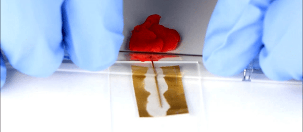
The researchers printed the circuit boards out of water-soluble PVA, with hollow channels in place of interconnects. After printing the boards, they injected a eutectic gallium-indium liquid metal alloy into these channels, populated the boards with components, making sure that their leads were in contact with the liquid alloy, and finally closed off the channels with PVA glue, which also held the components in place. When the board is ready to recycle, they simply dissolve the board and glue in water. The electric components tend to separate easily from the liquid alloy, and both can be recovered and reused. Even the PVA can be reused: the researchers evaporated the solution left after dissolving a board, broke up the remaining PVA, and extruded it as new filament.
Continue reading “A Solderless, Soluble Circuit Board”
indium6 Articles
Retrotechtacular: Manufacturing Philco Germanium Transistors
There was a time when all major corporations maintained film production departments to crank out public relations pieces, and the electronic industry was no exception. Indeed, in the sea-change years of the mid-20th century, corporate propaganda like this look at Philco transistor manufacturing was more important than ever, as companies tried to pivot from vacuum tubes to solid-state components, and needed to build the consumer electronics markets that would power the next few decades of rapid growth.
The film below was produced in 1957, just a decade since the invention of the transistor and only a few years since Philco invented the surface-barrier transistor, the technology behind the components. It shows them being made in their “completely air-conditioned, modern plant” in Pennsylvania. The semiconductor was germanium, of course — the narrator only refers to “silly-con” transistors once near the end of the film — but the SBT process, with opposing jets of indium sulfate electrolyte being used to both etch the germanium chip and form the collector and emitter of the transistor, is a fascinating process, and these transistors were quite the advance back in the day. It’s interesting, too, to watch the casual nature of the manufacturing process — no clean rooms, no hair nets, and only a lab coat and “vacuum welcome mats” to keep things reasonably clean.
As in most such corporate productions, superlatives abound, so be prepared for quite a bit of hyperbole on the part of the Mid-Atlantic-accented narrator. And we noticed a bit of a whoopsie near the end, when he proudly intoned that Philco transistors would be aboard the “first Earth satellite.” They were used in the radio of Explorer 1, but the Russians had other ideas about who was going to be first.
And speaking of propaganda, don’t forget that at around this time, vacuum tube companies were fighting for their lives too. That’s where something like this designer’s guide to the evils of transistors came from.
Continue reading “Retrotechtacular: Manufacturing Philco Germanium Transistors”
Circuit Boards You Can Stretch: Liquid Metal Nanomaterials Make A Strange Flex
If you think polyimide-based flexible PCBs are cool, wait until you get a load of what polymerized liquid metal networks can do.
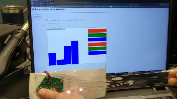
Seems like [CNLohr] has some pretty cool friends, and he recently spent some time with a couple of them who are working with poly LMNs and finding out what they’re good for. Poly LMNs use a liquid metal composed of indium and gallium that can be sprayed onto a substrate through a laser-cut stencil. This results in traces that show the opposite of expected behavior; where most conductors increase in resistance when stretched, pol LMNs stay just as conductive no matter how much they’re stretched.
The video below shows [CNLohr]’s experiments with the stuff. He brought a couple of traditional PCB-based MCU circuits, which interface easily with the poly LMN traces on a thick tape substrate. Once activated by stretching, which forms the networks between the liquid metal globules, the traces act much like copper traces. Attaching SMD components is as simple as sticking them to the tape — no soldering required. The circuits remain impressively stretchy without any apparent effect on their electrical properties — a characteristic that should prove interesting for wearables circuits, biological sensors, and a host of real-world applications.
While poly LMNs aren’t exactly ready for the market yet, they don’t seem terribly difficult to make, requiring little in the way of exotic materials or specialized lab equipment. We’d love to see someone like [Ben Krasnow] pick this up and run with it — it seems right up his alley.
Continue reading “Circuit Boards You Can Stretch: Liquid Metal Nanomaterials Make A Strange Flex”
Tearing Into A $1.3 Million Oscilloscope
Most hackers are rankled by those “Warranty Void If Broken” seals on the sides of new test equipment. Even if they’re illegal, they at least put the thought in your head that the space inside your new gear is off-limits, and that prevents you from taking a look at what’s inside. Simply unacceptable.
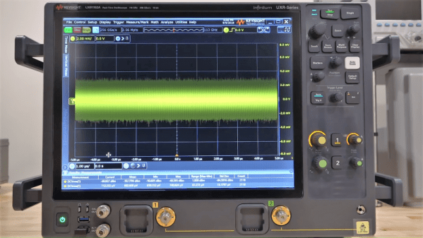
[Shahriar] has no fear of such labels and tears into just about everything that comes across his bench. Including, most recently, a $1.3 million 110-GHz oscilloscope from Keysight. It’s a teardown that few of us will ever get the chance to do, and fewer still would be brave enough to attempt. Thankfully he does, and the teardown video below shows off the remarkable engineering that went into this monster.
The numbers boggle the mind. Apart from the raw bandwidth, this is a four-channel scope (althought the unit [Shahriar] tested is a two-channel) that doesn’t split its bandwidth across channels. The sampling rate is 256 GS/s and the architecture is 10-bits, so this thing is dealing with 10 terabits per second. We found the extra thick PCBs, which are perhaps 32-layer boards, to be especially interesting, and [Shariar]’s tour of the front end was fascinating.
It all sounds like black magic at first, but he really makes the technology approachable, and his appreciation for fine engineering is obvious. If you’ve got even a passing interest in RF electronics you should check it out. You might want to brush up on microwave topics first, though; this Doppler radar teardown might help.
Solder At Room Temperature
Have you ever seen the science experiment (or magic trick?) where you get water supercooled to where it isn’t frozen, but then it freezes when you touch it, pour it, or otherwise disturb it? Apparently, ice crystals form around impurities or disturbances in the liquid and then “spread.” A similar effect can occur in metals where the molten metal cools in such a way that it stays melted even below the temperature that would usually cause it to melt.
[Martin Thuo] at Iowa University used this property to make solder joints at room temperature using Field’s metal (a combination of bismuth, indium, and tin). The key is a process that coats the molten metal with several nanolayers that protect it from solidifying until something disturbs the protective layer.
3D Printing With Liquid Metals
While 3D printers of today are basically limited to plastics and resins, the holy grail of desktop fabrication is printing with metal. While we won’t be printing out steel objects on a desktop printer just yet, [Collin Ladd], [Ju-Hee So], [John Muth], and [Michael D. Dickey] from North Carolina State University are slowly working up to that by printing objects with tiny spheres of liquid metal.
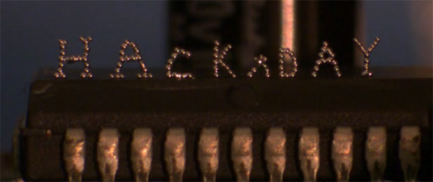
The medium the team is using for their metallic 3D prints is an alloy of 75% gallium and 25% indium. This alloy is liquid at room temperatures, but when exposed to an oxygen atmosphere, a very thin layer of oxide forms on a small metal bead squeezed out of a syringe. Tiny metal sphere by tiny metal sphere, the team can build up metallic objects out of this alloy, stacking the beads into just about any shape imaginable.
In addition to small metal spheres, [Collin] and his team were also able to create free-standing wires that are able to join electrical components. Yes, combined with a pick and place machine, a printer equipped with this technology could make true printed circuit boards.
Even though the team is only working on very small scales with gallium, they do believe this technology could be scaled up to print aluminum. A challenging endeavour, but something that would turn the plastic-squeezing 3D printers of today into something much more like the Star Trek replicators of tomorrow.
Video demo below, or check out [Collin]’s editing room floor and a vimeo channel. Here’s the paper if you’ve got a Wiley subscription.


