
Here at Hackaday HQ, we all have opinions about the way we like to do things. And no surprise, this extends to the way we like to lay out circuits in schematics. So when we were discussing our own takes on this piece on suggested schematic standards, it was maybe more surprising how much we did agree on than how much we had different preferred styles. But of course, it was the points where we disagreed that provoked the most interesting discussion, and that’s when I had a revelation.
Besides torturing electronics, we all also write for you all, and one thing we always have in mind is who we’re writing for. The Hackaday audience, not to blow you up, is pretty knowledgeable and basically “full-stack” in terms of the hardware/software spectrum. This isn’t to say that everyone is a specialist in everything, though, and we also have certain archetypes in mind: the software type who is just starting out with hardware, the hardware type who isn’t as savvy about software, etc. So, back to schematic layout: Who is your audience? It matters.
 For instance, do you organize the pinout for an IC by pin number or by pin function, grouping the power pins and the ADC pins and so on? If your audience is trying to figure out the circuit logic, you should probably go functional. But if you are trying to debug a circuit, you’re often looking at the circuit diagram to figure out what a given pin does, and the pin-number layout is more appropriate.
Do you lay out the logical flow of the circuit in the schematic, or do you try to mimic the PCB layout? Again, it could depend on how your audience will be using it. If they have access to your CAD tool, and can hop back and forth seamlessly from schematic to PCB, the logical flow layout is the win. However, if they are an audience of beginners, or stuck with a PDF of the schematic, or trying to debug a non-working board, perhaps the physical layout is the right approach.
Al Williams, who has experience with projects of a much larger scale than most of us self-taught hackers, doesn’t even think that a schematic makes sense. He thinks that it’s much easier to read and write the design in a hardware description language like VHDL. Of course, that’s certainly true for IC designs, and probably also for boards of a certain complexity. But this is only true when your audience is also familiar with the HDL in question. Otherwise, you’re writing in Finnish for an audience of Spaniards.
Before this conversation, I was thinking of schematic layout as Tom Nardi described it on the podcast – a step along the way to get to the fun parts of PCB layout and then to getting the boards in hand. But at least in our open-source hardware world, it’s also a piece of the documentation, and a document that has an audience of peers who it pays to keep in mind just as much as when I’m sitting down and writing this very newsletter. In some ways, it’s the same thing.
(And yeah, I know the featured image doesn’t exactly fit the topic, but I love it anyway.)


“For instance, do you organize the pinout for an IC by pin number or by pin function, grouping the power pins and the ADC pins and so on? If your audience is trying to figure out the circuit logic, you should probably go functional. But if you are trying to debug a circuit, you’re often looking at the circuit diagram to figure out what a given pin does, and the pin-number layout is more appropriate.”
PDF with things like actions and buttons, layers, and hyperlinks allows both representations to co-exist, so it doesn’t have to be an either/or.
Nut we first need a tool that does this, until then, merge request welcome I suppose.
I do agree though, though icanvas for kicad for one comes quite far …
How do you propose to do this? How is such a tool supposed to know which pins should be grouped together. Oh, I know – LET AI DO IT!! (Not.)
Huh? What now?
I was replying tt the message:
Not the quote above it. Sorry if I was not clear.
I.e. PDF has functionality that allows you to do hover/highlights, clickable items/links etc. Now we just need to generate said PDFs.
Also, actually in light to your comment, a symbol could always feature an (internal) default mapping that always relates to the used package. AI, or some smart logic, should be able to generate the nonfunctional schematic maybe?
Honestly, schematic capture rearranging is one thing where I could see “AI” being pretty good. You can always compare netlists to verify it’s the same.
…sure, I guess if the datasheets are be wrong. ;-)
heh i was not thinking of interactive elements but i was thinking the same thing that these often coexist.. i have a pile of microcontroller datasheets, and they typically provide one of each view. like the pinout is duplicated, once logically grouped and once physically grouped. the memory-mapped register layout is often duplicated in the same way, once by address and then broken out by function.
Yes! As someone with no visual memory or “mind’s eye” I find when I’m putting together a project (even just for myself) I need and want both views and sometimes additional ways of slicing the problem, since I’m using the CAD package as a sureogate mind’s eye too, e.g. when figuring out the best way to connect all N data lines of an SRAM chip where the order doesn’t matter and routing is all the main concern.
I suspect that it wouldn’t be too hard to do if one could solve the problem of storing any hints about arranging the schematic lines per view rather than globally. Essentially, then, the netlist stays the same between all views but the schematic symbols, line layout anchors/hints, and possibly net visibility could all be “per view”.
I’m fine with grouping pins by function on a schematic. I’m /not/ fine with having a pin-one marker on a box where the pins have been reordered, as in the illustration near the top of this article.
In a schematic, I prefer to group pins by function. That allows for much “clearer” schematics that are easier to understand and easier to spot errors on.
Good luck groupings pins by location of a BGA-package.
For debugging purposes, you can simply use the cross-probe functionality between schematic and PCB-layout. (present on any decent ECAD program).
The package is independent of the schematic symbol. A chip that comes in a BGA package should still be shown as a rectangle with pins grouped by their function. A whole generation, maybe two, has been polluted by “schematics” that just show the interconnections on a many-pin breadboard. Which BTW doesn’t work so well with BGAs, either.
Group by function makes more sense in an age where CAD layout programs can take over the job of pin routing. Unless one does their own manual layout — that may be a different story.
KiCad, and every other PCB design package I’ve used, has separate objects for the schematic symbol and the package footprint. Why would you need to see the package pin numbers in order when you’re drawing the schematic?
That previous topic about schematic standards / style was useful, but this it not much more then sand / salt / noise.
Schematics should always be drawn according to logical rules (mostly handled in that previous topic). And never according to PCB layout. Even when you are debugging, you first have to understand what you are debugging. And for that you need a logically drawn schematic. And before the “debugging” step, you have to design the schematic first, and then build the thing. Schematics are not just drawn for “debugging”.
Another clear indication for this is if you’re reverse engineering an unknown PCB. The first schematic draft you create from it (especially when done the old fashioned way with pen(cil) and paper is probably horrible, hardly any better then the PCB. Such schematics are usually drawn at least twice (Which is also where CAD is useful, as schematic sections can be untangled by dragging them around and reconnecting them.
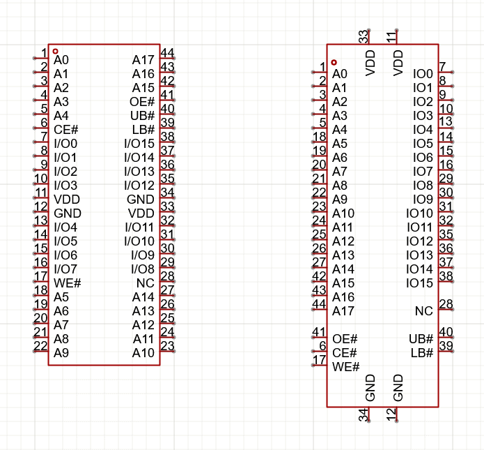
The RAM IC shown here is a good example. Just try to figure out it’s a RAM from the “pinout picture”. (I guess it’s a ram because I saw a WE# on the right picture. How many data and address lines does it have? How many Power and GND pins? How many “special” pins?
The symbol as used on the left side is normally never used in a schematic. The only reason it exists is because it’s generated from some sort of scripted approach, with data probably extracted from a PDF, or maybe some VHDL / Verilog code.
One thing that can be useful for debugging and as a learning tool, is to print out the leftside picture, and glue it on the IC. This works quite nicely with THT dip packages, (but SMT is too small for this).
For printing out such labels, I usually first put them in a spreadsheet. It’s easy to set a row height of 2.54mm , and set the columns to the width of the IC (use right / left alignment for the text).
I just did a little test in KiCad.
1. Put a (logically drawn) RAM IC on the schematic.
2. Hover and press [b]CTRL + e[/b] to load it in the schematic editor.
3. []Schematic Editor / Edit / Pin Table[/b]
4. Click on the [b]Number[/b] column to sort them numerically.
5. Copy the first half of the pins, paste them in a spreadsheet.
6. Click again on the [b]Number[/b] column to sort them in descending order.
7. Copy the other half, and paste these too in a spreadsheet.
This was pretty quick. Writing it down too more time then doing it.
I agree as well that he schematic should show logical layout. That’s what it is for.
I totally agree. Logical rules give a quick overview of what the circuit is doing. Part layout says absolutely nothing.
I have been drawing schematics for many decades, have been programming computers almost as long, and writing software/firmware for microprocessors and microcontrollers since their inception. Even when IEEE symbols came out, I still used standard symbols, but a few IEEE symbols for complex functions, like a 74123 do make some sense. But, again, it’s a logical symbol.
It is my humble opinion that people who are new to hardware NEED to learn logical layout, not just part pinouts. In the long run, it will end up making much more sense to them.
Also, I did not see that “agree to disagree” very much in that previous article.
Pretty much everybody agrees on the majority on the rules: Voltages up/down, signals left/right and such. There are a few areas where personal styles are different. (Such as where to place the decoupling caps). And apart from personal preferences, such things may also depend on the type of schematic.
Just to be clear: showing all decoupling caps in one corner of the schematic is useless. Put them at the IC pins. With any luck this helps you to remember where to place them in the board layout tool. But perhaps not, since you can’t see in the rats’ nest which of those capacitors is the one on pin 12 of the microcontroller.
Although you CAN add a field to each capacitor’s schematic symbol that shows which IC and pin that should be placed next to. So never mind.
I will usually place and connect the coupling caps to the appropriate pins in the schematic, but not connect the supply, then jump to a preliminary layout to places them using the rats nets, and then jump back the schematic and connect the supplies
Oh, why didn’t I think of this earlier? Everything would have been so much easier … thanks, I’ll keep that in mind.
That’s really pretty smart.
This is one of those minor details that people don’t agree about. To me, spreading decoupling capacitors all over the schematic is just a useless clutter that obfuscates the schematic more then it clarifies them. Decoupling capacitors are a necessary part, but they do not have any logical function in the schematic. I usually draw a long row of them just next to the voltage regulator, and when a schematic gets split into multiple sheets, then the first thing that moves to another sheet is all the power handling and decoupling capacitors. And the same for other “miscellaneous” stuff such as mounting holes.
Usage of decoupling capacitors is so basic in circuit design that I don’t even bother to add a note of how to use them. They just need to be there, and I assume the PCB designer (usually myself) knows what to do with them.
And it’s not always straight forward either. With logic IC’s (such as quad nand gates) the power supply is usually a separate unit (which also gets placed on the power sheet) and same for quad opamps and such.
With modern highly integrated stuff such as FPGA’s, there can be 20 or more decoupling capacitors for a single IC. If there are special needs for circuit decoupling (such as combinations of different sized decoupling capacitors), then it may be worthwhile to make some note on that in the schematic, or in other documentation. But making a note for each capacitor for which IC they go to is a waste of time.
One thing I have experimented with and that does work sometimes, is to use matching RefDes for IC’s and decoupling capacitors. So U42 gets C42. But quite often some IC’s need multiple capacitors, and there are also other (bulk etc.) capacitors in the power supply, and it’s more effort then it’s worth to attempt to stick to this rule.
To me it makes much more sense to just offload this to the PCB designer. At some point in the PCB design, you highlight all the power tracks and make a judgement whether decoupling is adequate. Sometimes a few decoupling capacitors get added, other times a few are removed.
Advantage of placing decoupling capacitors next to the related IC on the schematic is that you can see if you didn’t forget to add (or accidently deleted) some capacitors without counting all decoupling capacitors and ICs on the schematic, and you can see which capacitor belongs to which IC. Decoupling as row next to the power supply is useful for general decoupling spread around on the board.
Also, if you’re just sprinkling decoupling caps all over the place, you’re probably using all the same value and not considering how much is needed for each chip. Which is a pretty common practice, but kind of lazy.
Service manuals for complex gear do both: schematics laid out functionally, and then blow-ups of the PC boards, with test points etc marked. Sometimes there’s an overview section with simplified excerpts of the circuit being explained.
I actually don’t know what any of this means lol, I thought this was going to be an article for tips on content creation
This seems to argue for multiple schematics for a single project, depending on the audience or purpose. I would argue that such would be exactly the wrong choice.
If you have multiple schematics, you muddy the waters. People effectively must learn multiple standards. If, on the other hand, everyone learns to interpret the same schematic according to the “standard” (presumably, that standard exists on an organizational level in the commercial world), then everyone can speak and understand the same “language”.
And you don’t have to worry about “oh wait, which style of schematic is this? Is this the right one?”…
I can just hear the engineering calls:
“Yeah, that component on the lower right hand corner of page six. We need to change XYZ about that.”.
“There is no page six. Which style of the schematic are you looking at?”
Yeah, no. I’ll pass, thanks.
Grrr. That was supposed to be a top-level reply.
Sigh.
Take a look at the complete documentation of a colour tv from the early transitor models.
Atleast the european makers had a resonable standard which I consider good.
But it might be what I learned from 15 shelf meters of all schematics and documentation from all european radio and tv makers.
European Phillips was good example.
https://www.scribd.com/document/46984894/Philips-Ps1966c122-19e800-Service-Manual-7584
https://www.service-data.com/product.php/6856/16802/m16856?utm_source=chatgpt.com
Hopping into the comments to say (maybe uselessly): 1) I super enjoy reading the articles and comments on topics like this- most people in my life seem to act like I’m speaking a foreign language when I try to talk about things like the merits of one schematic layout philosophy over another 2) “The Hackaday audience, not to blow you up, is pretty knowledgeable…” that’s okay, for as many circuits as I’ve blown up it’s only fair that I be the target on occasion (okay…apologies for the bad/intrusive pun, I couldn’t help myself) 3) until the podcast/article I honestly hadn’t realized that there was two ways of structuring schematics because so much of my mental thinking immediately projects circuit diagrams into mechanical analogues that either tend to match the physical layout of the circuit or approximate it as some sort mechanical abstraction (maybe a product of getting my ME before my EE) -it’s honestly still hard not to think of wires as electric pipes even though I know better :-D
IMHO grouping pins by function is the way to go. Much easier especially for parts where grouping just sort of comes naturally. Everyone’s got their style tho. Do what makes sense to you :)
My opinion, but when I was a teen just getting into electronics, I was intimidated by even simple schematics, but I quickly picked it up when I realized their purpose was to break free of the constraints of physical construction, especially when trying to understand a circuit’s function or designing a circuit prior to building it. It’s MUCH easier. Long story short, schematics exist because they are intended to display their design function logically, and IC pins should be no exception. Components have their own data sheets showing pinouts and perhaps a schematic could include back pages showing physical layouts for reference. However, pin numbers can still be shown on schematics for that physical reference, just like CBE on a BJT, or transformer winding terminals etc are. Pin numbering layout on a DIP is pretty straightforward without needing a reference.