 There are a few possible ways to do a teardown of new electronics like the Apple AirTag 2 tracker, with [electronupdate] opting to go down to the silicon level, with die shots of the major ICs in a recent teardown video. Some high-resolution photos are also found on the separate blog page.
First we get to see the outside of the device, followed by the individual layers of the sandwiched rings of the device, starting with the small speaker, which is surrounded by the antenna for the ultrawide band (UWB) feature.
Next is the PCB layer, with a brief analysis of the main ICs, before they get lifted off and decapped for an intimate look at their insides. These include the Nordic Semiconductor nRF52840 Bluetooth chip, which also runs the firmware of the device.
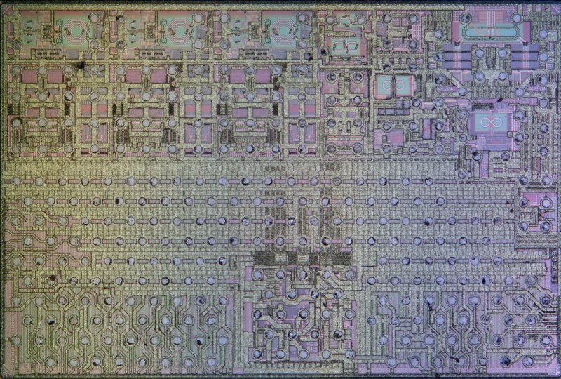
The big corroded-looking grey rectangle on the PCB is the UWB chip assembly, with the die shot visible in the heading image. It provides the localization feature of the AirTag that allows you to tell where the tag is precisely. In the die analysis we get a basic explanation of what the structures visible are for. Basically it uses an array of antennae that allows the determination of time-of-flight and with it the direction of the requesting device relative to it.
In addition to die shots of the BT and UWB chips we also get the die shot of the Bosch-made accelerometer chip, as well as an SPI memory device, likely an EEPROM of some description.
As for disabling the speaker in these AirTag 2 devices, it’s nestled deep inside, well away from the battery. This is said to make disabling it much harder without a destructive disassembly, yet as iFixit demonstrated, it’s actually fairly easy to do it non-destructively.


Wow, this is fascinating. I don’t see a battery, is there one?
There’s usually a 2032 in the center …
Hate on Apple all you will, I do believe they make excellent (looking) hardware and PCBs.
I rember an angry rant from Steve jobs, where engineers had to keep working to make inside also look nice. And I get that, highest quality standards.
Yeah, for all the stuff people hate about Apple rightly or wrongly, you can’t pretend that they aren’t about the peak of consumer hardware design especially under Jobs.
if you can’t even install non-signed apps or choose your OS on peak hardware, i guess your definition differs a lot than mine
That’s software not hardware
Guess you never heard some ‘notes’ people like Louis Rossman published about Apple hardware then.
But yeah, it looks nice, I agree with that.
In my experience this looks like a normal professionally designed PCB.
I have been in the PCB design industry for a few decades now, and the rule has always been that the board must look good for the customer to pay. It also makes you pay attention to detail.
I’m not an Apple fan, but they make nice looking stuff. I don’t like most of their hardware but it’s beautiful to look at and they put some thought into it. But it’s like a Toyota FJ40 and a Rolls Royce Cullinan. Both can go off-road but the ideas behind the two are entirely different. I need a rugged phone I can drop, with a battery that can recharge an iPhone several times. And I don’t like to pay Apple prices either.
The only hardware I’d love to own are Airtags. I wish they were available for Android users. The alternatives I’ve seen so far just aren’t great. The Google find my network is so limited that it just fails. The Google network just doesn’t work right. It can take days for your tag to move.
If Airtags worked with Android I’d buy a bunch of them.
Last time I was on a plane, I was bored and started looking into the different Android settings, and came across some menu that allowed me to scan for tracking tags. It immediately found a few air tags on that flight, and game me also the option of making them beep.
I am not sure how to get to those settings now
Apple is a decent company but they’ve not mastered zero point free energy. Note the large round hole in the center of the PC board :-)
https://www.youtube.com/watch?v=KEuqIs4RIEA
Cheers.
The video/photos really need some sort of scale to them, from the thumbnail the PCB doesn’t look particularly impressive until you realise the largest thing on there is maybe 3x5mm.