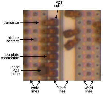
Although not as prevalent as Flash memory storage, ferroelectric RAM (FeRAM) offers a range of benefits over the former, mostly in terms of endurance and durability, which makes it popular for a range of (niche) applications. Recently [Ken Shirriff] had a look inside a Ramtron FM24C64 FeRAM IC from 1999, to get an idea of how it works. The full die photo can be seen above, and it can store a total of 64 kilobit.
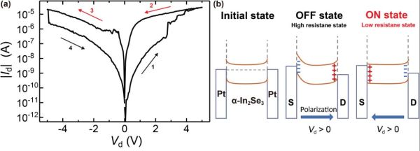
One way to think of FeRAM is as a very small version of magnetic core memory, with lead-zirconate-titanate (PZT) ferroelectric elements making up the individual bits. These PZT elements are used as ferroelectric capacitors, i.e. the ferroelectric material is the dielectric between the two plates, with a positive voltage storing a ‘1’, and vice-versa.
In this particular FeRAM chip, there are two capacitors per bit, which makes it easier to distinguish the polarization state and thus the stored value. Since the distinction between a 0 and a 1 is relatively minor, the sense amplifiers are required to boost the signal. After a read action, the stored value will have been destroyed, necessitating a write-after-read action to restore the value, all of which adds to the required logic to manage the FeRAM. Together with the complexity of integrating these PZT elements into the circuitry this makes these chips relatively hard to produce and scale down.
You can purchase FeRAM off-the-shelf and research is ongoing, but it looks to remain a cool niche technology barring any kind of major breakthrough. That said, the Sega Sonic the Hedgehog 3 cartridges which used an FeRAM chip for save data are probably quite indestructible due to this technology.


