Growing A Gallium-Arsenide Laser Directly On Silicon

As great as silicon is for semiconductor applications, it has one weakness in that using it for lasers isn’t very practical. Never say never though, as it turns out that you can now grow lasers directly on the silicon material. The most optimal material for solid-state lasers in photonics is gallium-arsenide (GaAs), but due to the misalignment of the crystal lattice between the compound (group III-V) semiconductor and silicon (IV) generally separate dies would be produced and (very carefully) aligned or grafted onto the silicon die.

Naturally, it’s far easier and cheaper if a GaAs laser can be grown directly on the silicon die, which is what researchers from IMEC now have done (preprint). Using standard processes and materials, GaAs lasers were grown on industry-standard 300 mm silicon wafers. The trick was to accept the lattice mismatch and instead focus on confining the resulting flaws through a layer of silicon dioxide on top of the wafer. In this layer trenches are created (see top image), which means that when the GaAs is deposited it only contacts the Si inside these grooves, thus limiting the effect of the mismatch and confining it to within these trenches.

There are still a few issues to resolve before this technique can be prepared for mass-production, of course. The produced lasers work at 1,020 nm, which is a shorter wavelength than typically used, and there are still some durability issues due to the manufacturing process that have to be addressed.

Digital Attenuator Goes From Manual To Arduino Control

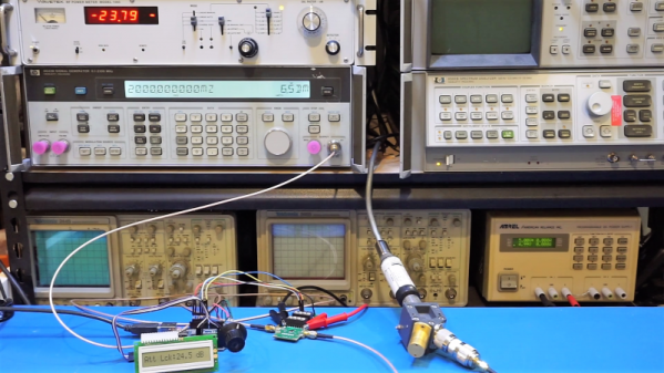
[Kerry Wong] comes across the coolest hardware, and always manages to do something interesting with it. His widget du jour is an old demo board for a digital RF attenuator chip, which can pad a signal in discrete steps according to the settings of some DIP switches. [Kerry]’s goal: forget the finger switch-flipping and bring the attenuator under Arduino control.

As usual with his videos, [Kerry] gives us a great rundown on the theory behind the hardware he’s working with. The chip in question is an interesting beast, an HMC624LP4E from Hittite, a company that was rolled into Analog Devices in 2014. The now-obsolete device is a monolithic microwave integrated circuit (MMIC) built on a gallium arsenide substrate rather than silicon, and attenuates DC to 6-GHz signals in 64 steps down to -31.5 dBm. After a functional check of the board using the DIP switches, he whipped up a quick Arduino project to control the chip with its built-in serial interface. It’s just a prototype for now, but spinning the encoder is a lot handier than flipping switches, and once this is boxed up it’ll make a great addition to [Kerry]’s RF bench.

If this video puts you in an RF state of mind, check out some of [Kerry]’s other videos, like this one about temperature-compensated crystal oscillators, or the mysteries of microwave electronics.

Continue reading “Digital Attenuator Goes From Manual To Arduino Control”