One downside of working with the old Inmos Transputer devices is the rarity and cost of the original silicon. Obviously, you can’t sidestep the acquisition of the processor—unless you emulate—but what about replacing the IMS C011/C012 link chip? You need this (expensive) part to interface the transputer to the programming host, but as [Erturk Kocalar] discovered, it’s perfectly possible to coax a Teensy to do that job for you just as well.
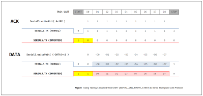
Transputers work by utilizing an array of bit serial interfaces to connect a network of devices, allowing for cooperative computation on tasks too large to fit on a single device. This protocol is, at its link level, a simple asynchronous bit serial affair, with 11-bit data messages, and a raw two-bit frame for the acknowledge. The C011 device at its heart is just a specialized UART—it takes 8-bit parallel data from the host, dealing with handshaking, and pushes it out to the first transputer in the chain at 5, 10 or 20 Mbps, but inverted and with two start bits and a single stop bit. In parallel, it performs the same task in the reverse direction.
[Erturk] realized that the Teensy UART has an inverted mode and, crucially, a 9-bit data mode. This allows the second start bit to be generated as bit 0 of the word, with the remaining eight bits forming the payload. Simple stuff. Additionally, the Teensy UART is capable of the maximum transputer bitrate of 20 Mbps, without breaking a sweat.
Continue reading “Putting A Teensy To Task As A Transputer Link”

![An Inmos RAMDAC (the 28-pin DIP) on the motherboard of a 1989 IBM PS/55. Darklanlan [CC BY 4.0]](https://hackaday.com/wp-content/uploads/2019/03/ibm_vga_90x8941_on_ps55.jpg)


