If you read my first post about a simple CPLD do-it-yourself project you may remember that I seriously wiffed when I made the footprint 1” wide, which was a bit too wide for common solderless breadboards. Since then I started over, having fixed the width problem, and ended up with a module that looks decidedly… cuter.
To back up a little bit, a Complex Programmable Logic Device (CPLD) is a cool piece of hardware to have in your repertoire and it can be used to learn logic or a high level design language or replace obsolete functions or chips. But a CPLD needs a little bit of support infrastructure to become usable, and that’s what I’ll be walking you through here. So if you’re interested in learning CPLDs, or just designing boards for them, read on!
The design itself tries to utilize through-hole parts and a socket for the CPLD so that you could more easily build it yourself without a lot of surface mount soldering. With that said, the oscillator is a surface mount device (SMD) just due to the cost and size of its through-hole counterpart.
I also added a USB Mini connector to make it easier to power the assembly, like when making a video for Hackaday. I am only partially happy with the USB connector approach as it is useful only for the 5V version and dangerous if the 3.3V CPLD is used. I also added a two-pin connector for power at the last minute but really would like to have added a diode to protect against reverse polarity.
In addition, an external clock source may easily be applied via a connector thanks to a suggestion/comment from the last post.
Project Files
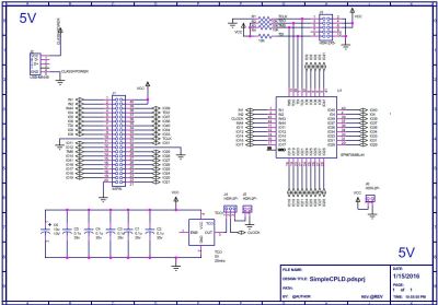 Looking at the schematic you can tell there isn’t much to it: basically the CPLD, the circuit for in-circuit programming and an oscillator to drive the logic in the CPLD.
- Simple CPLD R2 Schematic
- Simple CPLD R2 PCB Layout
- Simple CPLD R2 BOM
- Gerber Files Simple CPLD R2
- Gerber Files Simple CPLD R2 (OSH Park Compatible)
- Simple CPLD R2 Proteus CAD Project
- CPLD R2 Quartus Design Files
- Altera Quartus 9.1 Web Edition (Free)
The project can also be found on Hackaday.io
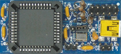
The CPLD: A surface mount part that fits a through-hole socket
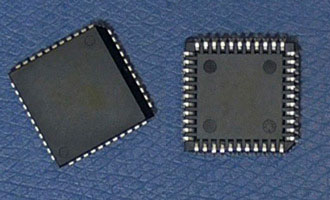 This part known as either the EPM7032 or EPM7064, comes in a 44 pin plastic leaded chip carrier (PLCC) which is sometimes called J lead due to the J shape of the pin leads. This package can be inserted in a through-hole socket or directly soldered to the PCB.
These parts tend to cost $8-$9USD from the standard catalog sources. I have a batch coming from overseas at a much cheaper price, if anyone is looking to build several units where a cheaper source pays off then message me.
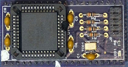
The Oscillator
The original on-board oscillator is a 25 MHz device, mostly because “fast” is usually good. In real life I think a 4 MHz or a special frequency such as 14.318 MHz (NTSC x 4) or 1.8432 MHz (UART) may be more useful for slower logic as the clock does not need to be divided down as much. With that said, it’s easy to use a different TCO or to apply an external clock to the pins provided.
Programming the CPLD
The 10 pin connector and a handful of resistors comprise the programming circuit, this footprint is often called the JTAG connector.
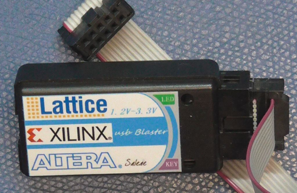 To program a standalone CPLD like this one, a dedicated programmer is needed. An approved “Altera USB Blaster” costs $50 and is available from places like Digikey. I have several clones that I got off of eBay including one that is a clone that supports Altera, Xilinx and Lattice all in one.
Down the road I hope to do a programmer clone project, the parts are sitting on the table next to me.
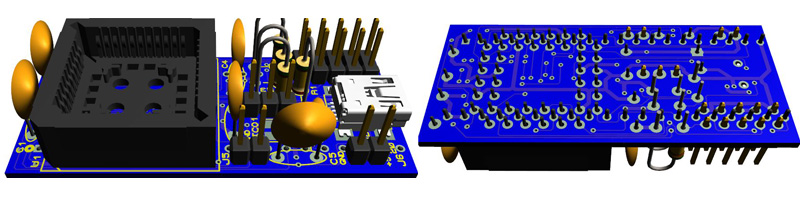
The PCB
 The PCB is a simple two-sided design, however assembly requires first installing the 40 position “machined” pins from the bottom, clipping the leads short, and then installing the socket from the top.
The 3D View
Lots of I/O
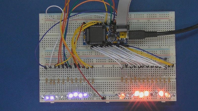
The first thing that jumps out when using one of these CPLD modules is the large number of Input/Output (I/O) lines available from the 40 pin package, 35 I/O lines to be exact. There could have been more except I like to make sure there are several ground pins. As the name implies, I/O lines can be programmed to be inputs, outputs or bi-directional and can also tristate and simulate open-collector outputs.
The other feature of a module like this is the speed; it switches in nanoseconds instead of the microsecond speeds found in many microcontrollers.
The CPLD Design
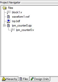 The entire design contains all of the files needed to quickly utilize the Simple CPLD board including the pin and device assignments. To use this design, download Quartus Web 9.1 and install. Download the design, unzip and open the project Simple-CPLD-Demo.qpf. Click on the Files Tab under Project Navigator and you should see the three important files:
- top.bdf – The top of the project as a graphical block diagram file (bdf)
- block1.v – The Verilog file for the symbol named
block1o. the bdf - waveform1.vwf – The waveform that drives the simulation
The lpm_counter0.qip file was installed automatically by the compiler.
The Schematic (bdf)
Clicking on top.bdf brings up the top sheet. I still make the top sheet a graphical sheet but you could forego this and use Verilog or VHDL. (I used to use AHDL 25 years ago)
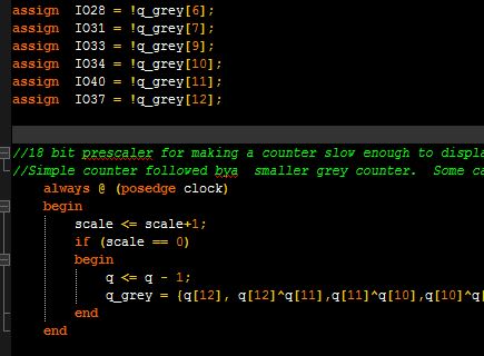
On the schematic we see a functional block aptly named block1 that represents the Verilog file underneath it. Shown are also are the pins representing the chip pins themselves.
Assignments
 Click on Assignments, Device to select whether you are compiling for the 32 or 64 macrocell device.
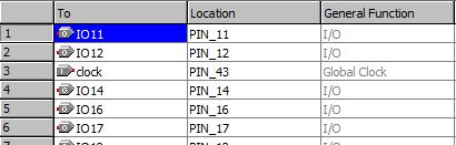
Click on Assignments, Assignment Editor to see the pin name to pin number assignments. Again I name the pin in a way that makes it easy to assign the pin number, I.E. IO11 is Pin 11.
The Verilog File
 On the top.bdf file, double-click on the symbol
 block1 and the underlying Verilog file is opened in a text editor. The built-in text editor is pretty reasonable, however a lot of use like to assign an external editor, in my case I use Notepad++ with the Verilog colorizer tweaked to my own preference for colors.
Here all of the assignments have been made to match the block to match the project to match the PCB.
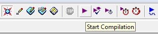
Compiling
Click on the purple “play” button to compile the design.
Simulation
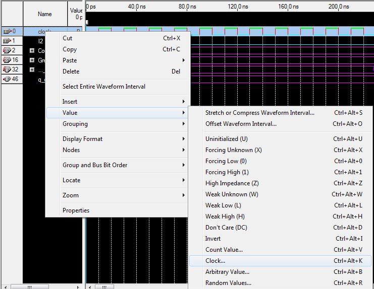 Click on the file waveform1.vwf and the input to the simulation will be opened in the waveform editor. (I have mine preset to use pretty colors). The only input to the demo is the clock. To change the clock’s timing as an example, right click on the clock waveform and select Value, Clock, and change the clocks frequency and duty cycle.
Simulation
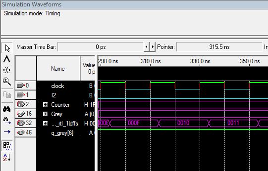
Click on the Simulation Icon and the resulting waveform should open up with the results of the simulation of the design, a couple of counters in this case.
![]()
Programming the CPLD
Plug your programmer into the 10 pin JTAG connector noting the Pin 1 locator dot on the PCB which should line up with Pin 1 on your programmer plug or the Pin 1 stripe on the cable itself.
![]()
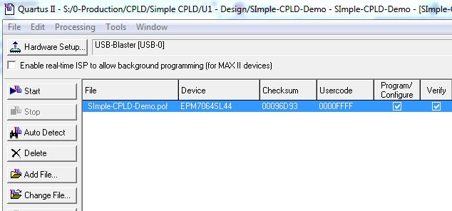
Once satisfied with the output, or if you’re the adventurous type and want to jump straight to trying the design on actual hardware, simply click on the Programmer Icon. You should see your programmer listed (USB-Blaster here) and the file Simple-CPLD-Demo.pof and the device you selected earlier. If it isn’t present, click Add File and select it. Select the checkboxes for Program, Configure, and Verify and click Start.
If everything works correctly you should see a message about the success in the ever-present message box and in my case my LEDs started to blink.
Conclusion
I wanted to demonstrate a beginning-to-end experience for the beginner. Starting with this Simple CPLD module you can be up and running in a few minutes. You can also start learning/editing Verilog using the file provided or replace or add graphical components to the top sheet if you would rather design using a schematic.
The CPLD is electrically erasable meaning you can reprogram it over and over and in between it will retain the configuration unlike many FPGAs that have to be programmed every power cycle, making it ideal for small and medium size application. Build along and have fun!


Once you’ve got one SMD part, you might as well have all SMD parts. Especially when that one is a non-trivial 4-pad component (compared to R or C)
Both SMT parts _can_ be omitted if need, there is a power and clock connector to supply via through-hole pins.
Agreed. Just get yourself some really sharp thin tweezers and you’ve got the most important tool to solder an SMD part with almost any soldering iron <60W there is.
I use an X-acto #11 blade. The sticky flux and/or paste and the small lightweight parts make it easy to pick them up. They’re awesome for holding down those pesky resistors while soldering to avoid tombstones. Once I got used to surface mount parts, I find I don’t want to deal with through holes parts, such as drilling the PCB or reworking.
The blades are cheap but watch for that flying brittle tip if you’re too rough.
I’ve got tweezers for the bigger SMT pieces, but I’ve gotten skilled enough with the blade that it’s a non-issue.
Heh, a good magnifier is one of my main tools (my eyes probably aren’t as good as yours). For me the other basic tools are good curved tweezers, flux (I use no-clean and tacky) and I keep some of the orangewood sticks handy for holding down as well as lintless chemwipes and alcohol for cleanup. It starts to get harder if you have to desolder a part as now you have to get multiple pads soft at the same time and tweezer solder irons or hot air starts to really help (a whole video on this actually and what fun a halogen bulb can be). Once getting into parts with pads underneath or fine line then paste starts to be required.
So some SMT is easy, some harder, some very specialized. Sometimes a socketed part can be a whole lot easier for playing as you can easily change the part if you blew it up or think you blew it up.
Fully agree on socketing, especially for something like this. However, surely there are smt plcc sockets?
The idea was to offer a kit-like design that could easily be soldered by a home hobbyist. Also the SMT socket would probably preclude the chance of inter-spacing the bottom pins. :)
Should a metal ash tray, filled with sand, on top of a hot-plate be a decent replacement for hot-air if all the parts are on the top-side of the board?
I have seen camera stabilising circuitry, added to cutlery for people with Parkinsosn’s (hand tremors). Has anyone ever hacked this into a soldering iron?
For projects like this, with just a few token SMD parts, that would be nice…
Nice! If this was availible in the hack a day store I would snap this up immediately!
You can get the PCBs made at Oshpark and parts from Digikey or I have a couple at herdware.com I could put some up in Tinde I reckon (now that we are family). Anyone wanting just the PCB I can drop in the mail for no-charge while supplies last.
Thanks for making the PCBs available. I think I’ll order a few from Oshpark.
Okay Bill, I’ll bite. I would like to have one if you have any left.
I can be reached on the Hackaday.io
I’d also take one if you have any left. Very cool stuff!
A version of the board that skips the through hole socket might be nice – I find PLCC very approachable, and knocking a dollar off never hurts.
Yeah there is a “real” board possibility in the future, I would re-evaluate which manufacturer would be best and which architecture.
If you do that, could I suggest looking for a smt PLCC socket with compatible footprint to the relevant PLCC chips? Two designs in one has always struck me as desirable.
Also if you saw the vid I complain about the cost of these in the “standard” supply companies and have some overseas parts coming. Once going to full SMT then cost would be a pretty critical selector.
Why still developing PTH boards? IMHO a waste of time and PCB space. Also having the header pins in between of the plcc socket is not hobbiest friendly nor reliable.
A TQFTP-44 and 0805 can be soldered with almost every solderingiron with no special tools, except flux.
We’ll get there, I am doing the crawl before walk approach for hobbyists.
Awww, pshaw. There’s haters, especially here Bill Herd. Just ignore them and keep up the awesome work :)
Thanks. Electronics is a wide field and depending on where someone is some approaches don’t make sense relatively speaking. Surface mount is just one of those doozy steps, already we have seen tqfp-44 trivialized and a 4 pad part non-trivialized in just a few posts. I really don’t know what percentage of hobbyists are capable/comfortable with SMT and for which it’s a deal breaker. Here I was hoping to bleep over the issue and get to the fun part of programming! Thanks again. Bil
From a signal integrity point of view, it make no sense to continue on the through hole parts. The use of through hole parts adds a lot of parasitic – the extra long lead frame, long pins, socket parasitic, long thing traces, loop area, and the location of the decoupling cap.
The edge rates of the parts are getting faster and faster and you just can’t built thing like in the 1970’s any more without doing your signal integrity homework. Let’s say this board is not setting a good example.
I thought SMT would be hard until I tried it. It’s easy.
Spoken like someone who does not know Bill Herd’s history.
If I knew him PTH would be ok? :S
I just want to say
– SMD parts are generally smaller
– their ‘legs’ (pads) don’t occupy both sides
– they are easier to solder if you have a small bit experience.
– In general there are more parts to choose from then PTH.
Also particular to this board the header interferes with the socket of the PLCC (they are in the same area) which would cause shorts between pins. He did lot of tricks to make it breadboard friendly which is ok (the breadboard part) but IMO it would be easier and more reliabler with SMD parts then PTH parts…
The socketed CPLD means we can use it for development. One board 200 programmed CPLDs. Actually the socket probably will not last for 200 insertion/removals, but still for a few parts a good design.
And its re-programmable. :)
A long way from the old day when a prototype board was huge. As I recall, the proto C128 used a lot of large boards.
Ya, we called the thing “the barn door”, when really it was the thing you would prop the barn door open with!
I believe Gray coding is named after Frank Gray — a proper noun — and unrelated to the different regional colour spellings.
I noticed you spelled color “colour” :) Your right of course, I just don’t trust myself to remember which is which this late in life.
Beautiful video nonetheless, you’ve been a great inspiration to finish many of my digital projects I would’ve otherwise never attempted. FPGA’s for me are a step in the right direction, but generally overkill for something that can be easily done with a cheaper/simpler CPLD on the BOM.
Not that I use solder-less breadboards, but it was great to see the toolchain and schematics in such a complete overview.
Hey Bill, isn’t the PLCC socket missing from the list parts? By the way, nice project, i would like to try it out! :)
Ack, I will get that fixed. I took a shortcut on the whole socketed thing and its actually the CPLD that’s missing. :) (I swapped part numbers) I have to figure out a way to get both to show up in the 3D view also.
You’re not missing a bunch of terms in the AND/OR array, are you, Bil? Probably not; you used Verilog instead of the copy machine on this “gate array”…
/Old Commodore joke that people who didn’t read “On the Edge” or don’t know Commodore people won’t get…
ROFLOL… that guy photocopied the very complex piece of paper crooked and never looked back. Probably wouldn’t have been a C128 if he hadn’t (It was called something else prior)
Actually, that was Dr. Cong Su that missed a row of terms in his gate array, not Bil, but Bill fixed it for him. See pg 354 of “On the Edge”.
Hey Bil, great build! Have you ever used any (not knowing the proper terminology) edge header designs? Here’s one method that uses right-angle pin headers, one row long and one row short. The edge of the board goes in the trench of the breadboard. Since the PCB is vertical it isn’t as crucial that you constrain the width.

Neat! I thought of doing this before but couldn’t find anything at the time long enough to reach.
I ended up using right pin headers on one edge and chopped an IDE cable and soldered the leads to the other side. I jammed in a set of straight headers into one row of the connector and plugged it into the breadboard that way.
It worked but it was a fricken hassle soldering all those wires and getting them in the right order.
Interesting. I would not have thought to find two different lengths of the right angle connector.
I’d suggest using the two-row stuff, and then using a snap-off piece of board to convert the size. A DIL female header, two SIL pin headers to either size, and you’re set. You could probably go with a board-edge connector too, if you can find one that’ll fit.
I came here to make this suggestion. You can put _massive_ breakout boards / submodules (e.g. CPU, FPGA, complex IO thingy, etc) into a breadboard with this technique.
Hi Bil, as usual I enjoyed reading your articles/builds/logs. I often find that most boards only leave one or two rows of exposed unused pins when plugged into a breadboard, so I’ve start to use 2 breadboards side by side with/without the power rails in between thus only using a single row of pins.
http://i.imgur.com/MG7Sli0.jpg
I have a couple set up this way. You have to be careful not to “pop” the bread boards when inserting some wider modules. After I busted the pins on a hard to repair board, I finally took some scrap lumber and screwed the breadboards in position, relative to the other. The boards don’t pop up and the PCB isn’t the only thing holding the breadboards in place.
Yes I agree, though if someone made spacers in multiples of the pin spacing and using the same interlocking mechanism that would things so much easier.
Re: two different pinheader lengths, and the vertical mounting. Awesome hack! Will use.
I actually learned CPLD basics with an Altera 7064 in an edge-header breakout board like this.
Do they still make 5V Altera CPLDs? Pozdrawiam thought they stoppedm making them awhile ago.
Yes the EPM7064S is 5V the EPM7064A is 3.3V but 5V tolerant inputs. This means that it would work to drive 5v TTL but not 5V CMOS unless an open drain is used with pullup. (Per the video on CMOS and TTL levels :)
Looks good and it must have been an effort to get those pin through parts to all fit.
I have made a number of different types of CPLD prototyping ‘boards’. Most of them plug into each other Arduino shield style.
Breadboard is good to but I think you would have to move to a single sided approach with larger 88 / 100 pin chips. I have seen 88 pin PLCC sockets but never a 100 pin.
QFP44 is easy to solder (0.8mm). Up to 100 pins is ‘doable’ but it gets hard to hand solder by 0.5mm.
Anyway here is what I would have done differently –
1)
Your pin width is the standard 0.6″ like a ‘wide’ DIP IC. On a bread board it could plug right over the top of a ‘narrow’ DIP IC (0.4″). So you can stick something like a SRAM chip under the CPLD and have control the SRAM.
The pins of the CPLD that connect to the VCC and GND pins of the SRAM chip can be programmed as inputs. You loose two CPLD IO but gain a lot of convenience and some other benefits like being able to run much higher bus speeds to the smaller chip because you don’t have ruddy long wire acting like antennas.
The limitation of this design is that you have ground pins in the middle and they are not likely to allow you to do what I just described. I would put ground / VCC at the ends of the DIP connector to make the module more versatile and useful for higher signal rates on a breadboard.
2)
Also, CPLD’s are *FAST* and 25MHz is slow! The real problem is that a poor PCB design wont work at higher speeds. Moden FPGA has internal PLL oscillators so that you can use a low speed xtal which is not so sensitive to PCB design and at the same time operate the internal at more FPGA like speeds.
You can get a 50MHz XTAL to work quite easily. I use 50MHz even with single sided boards.
100MHz will be a bit harder but is doable.
you would have to ‘loose’ the jumper block or leave it underpopulated unless required because the two little 0.1″ jumper pins will be like little antennas. Perhaps you could experiment with two sources going though two resistors and have a jumper to ground to kill the unwanted source. I can’t see series type jumpers working but at the same time I have never tried.
There are lots of app notes on this. Generally my approach is – surround the RF link to the CPLD with ground pours and keep a good clearance between the RF link and the ground pours to reduce shunt capacitance.
Jumper pins? Oh come on, the wavelength is like 3m at 100MHz. An 8mm pin header ain’t doing jack but the routing to it could be problematic if it introduces an inductive loop.
You can forget making off-board connections at those frequencies unless they’ve all got their own ground or are differential pairs… but that’s not the fault of the poor maligned little jumper pin.
The Terasic USB Blaster clone costs $50. The original one from Altera costs way more.
Yup, love Terasic, they have me listed on their website. Overseas clones are also available for cheaper yet though I guess there is a copyright issue with identifying as a USB Blaster (which strangely enough is the only one the software will use). I DO want to do a multi-vendor ISP programmer as a project tho…..
It’s always about the software.
There’s a lot of hardware, like cheap JTAG programmers, logic analyzers, microcontroller programmers, that could theoretically be used to program those chips, but nobody has ever written a firmware for this.
Recently I saw laptop analyzer tool on amazon and in picture the board has Altera MAX on it (http://www.amazon.in/Laptop-Analyzer-Tester-Notebook-Buyyart/dp/B01BGLK40W/ref=sr_1_1?ie=UTF8&qid=1454653999&sr=8-1&keywords=laptop+analyzer) and I searched more on ebay(http://www.ebay.com/itm/Laptop-PC-Computer-PCI-Motherboard-Diagnostic-Tester-Analyzer-Post-Card-USA-/111241488409) it has xilinx cpld(xc9536xl) on it comes with nokia lcd display, can we use these board anyway they are incredibly cheap.
I always wanted to work with CPLDs and FPGAs, but I didn’t since university. The thing is, that I never met a real world problem, that I could’ve solved better/faster/cheaper/more reliable with programmable logic, than with a combination of microcontroller, analog electronics, classical digital logic, and mixed-mode ASICs.
Somewhat sad, but when you design for mass production, programmable logic can nearly never meet the price target.
I saw laptop analyzer board on amazon (https://www.amazon.in/gp/aw/d/B01BGLK40W/ref=mp_s_a_1_1?qid=1454679472&sr=8-1&pi=AC_SX110_SY165_FMwebp_QL65&keywords=Laptop+analyzer) it has Altera MAX on it and it is very cheap so I searched more is board on ebay with xilinx CPLD, can such a board can be used as cheap development board.
” it switches in nanoseconds instead of the microsecond speeds found in many microcontrollers”
Is that the GPIO speed, or internal transistor switching speed?
Hi May I know what software did you use to draw the schematic of the CPLD?
Hi, i just came across this project and wanted to see how fare i come.
I tryied to download the Quartus II Web Edition 9.1 but it is no longer available. I searched the Intel website where they say that version 13.1 is the latest version which handles the Max 7000 series, there was also a device file to download. I tried it out, but i just loads the devices for Max II and V.
Can anybody tell me if there is a way to work with this chips today?