Staking and potting are not often used in the hobby electronics world, not really entering to the common vernacular. However, everyone who’s ever busted out a glue-gun to convince that dang wire that keeps coming loose to stay has done it.
However, as [Sean Thomas] touches on, staking is not necessarily as easy as a dob of hot glue. There is a method to the madness. [Sean] gives some examples in pictures, but also directs people to the excellent NASA standard methods for staking. It’s surprising how many unintuitive caveats there are to the proper technique.
Potting, or covering everything in epoxy forever, is a great way to get a waterproof, unserviceable, and practically mechanically invincible circuit. The big challenge in potting is picking the right material. A soft silicone, for example, might transfer an unexpected force to an unexpected section of the circuit and cause a mechanical failure. A nice hard epoxy may be too insulating and cause a thermal failure. The standard RTV from the big box store has acetic acid that will eat your components.
These two techniques that come in handy when you need them and worth the bit of reading it takes to get familiar. Have you used either in your own workshop? Let us know the application and the material/techniques you have tried in the comments below.


I would hesitate putting waterproof and epoxy in one sentence, some do take up water and thus can cause corrosion…
Silicones do much better in waterproofing, but you need to be aware of the curing system and it’s limitations.
Are there still companies out there that use potting to prevent their stuff being reverse engineered?
There are. And honestly, it does the job. I tried to decap, and the epoxy bond to the component was harder than the solder bond. I ended up with a bare PCB and potted components still embedded in the potting.
Hot H2SO4 drop would do the job.
Hot water (read boiling) softens epoxy a lot, without the destructive effects of strong acids ;-)
That is true, if you basically want some silicon to survive. If it is a populated PCB, dropping some acid is probably not the way to go.
It worked for Steve Jobs!
There’s some I’ve come across seem practically like glass, tools skid off them.
Though come to think of it, they might be a bake on type.
Perhaps it’s also bake off :-) With enough heat it has to surrender.
I’ve recently found that a temperature controlled soldering Iron is a very useful tool for digging through epoxy potting. It’s not hot enough to melt or burn the epoxy, but the heat reduces it to the consistency of hard jello so you can easily dig out a component for testing or replacement. Only done this with transparent epoxy, working blind digging into opaque epoxy would be much harder.
Last year I tried to reverse a mold CCA that was out of production (because the original supplier was out of business) The dang thing was also inside a metal tube, which I first had to mill a slot, then peel it off.
The PCB was ceramic, and though I did not peel off components, it proved nearly impossible to trace out, compounded by the fact it broke into 3 pieces.
I hate potting. It makes it impossible to repair the device…
In the Solectria electric vehicles I repair: http://www.wolftronix.com/EV.htm
They use custom Vicor DC-DC converter bricks to convert the 144V to 12V to run the rest of the car accessories.
They are dying due to the age of the capacitors in them, and they can’t be repaired because of the potting.
If anyone has any Vicor DC-DC converter bricks (100-200V in 12V out), and are willing to sell them let me know.
Otherwise, when I get some free time I will have to design one a replacement…
Sound like the kind of thing I’d make custom hole saws for.
There’s guys out there that will dig eproms out of potted ECUs to upgrade them.
They are zero current switchers, the capacitor(s) that are in series with transformer primary fails shorted. This causes the input fuse to pop.
I have a few bad ones I can send you, If you want to attempt to repair them.
But, then again, I can still buy them at rather optimistic prices:
http://www.digikey.com/product-search/en?keywords=1102-1229-ND
Or much cheaper on eBay when they turn up. ;)
Replace “impossible” with “not economically viable.”
But, if it was not potted, I could just replace the bad film caps.
I was trying to reverse engineer a commercial LED control circuit that failed, they didn’t pot it but sanded off the markings on the IC! Maybe that’s why it failed haha. Saw another LED control circuit that was fully potted. LED control seems to be very proprietary it looks like
Yeah, it is almost like they really don’t want you to fix repair stuff:
http://www.wolftronix.com/umoc340_15/images/IMG_0188.jpg
It appears to be some sort of advanced Romulan technology…
Tire pressure sensors are absolutely encased. For good reasons though.
Don’t use tin cure RTV. Use platinum cure. Most platinum cure RTV silicones have essentially zero shrinkage while most tin cure ones shrink some. Most tin cures need to be post cured with heat to complete their curing. Tin cure RTV tends to deteriorate over time. Platinum cure has an indefinite shelf life. Tin cure RTV inhibits curing of platinum cure RTV, but not the other way around.
Tin cure isn’t enough less $ than platinum cure to justify bothering with its disadvantages.
I’ve used hard urethane resin for potting. Made some red LED turn signals for a 1941 Hudson pickup truck and potted the LM317 voltage regulators, resistors and the LEDs in the urethane housings I cast from the same resin. I deadbugged the circuits and for 12V connection I simply used male and female 1/4″ spade connectors poking out of the back end of the potting.
There are also thermal 2 part expoxys. They have a very high heat transfer rate. Used it to pot high current diodes.
I need a material that I can use to protect SMT components (resistors, caps, ICs) from mechanical shock, but that component also needs to withstand 200 C for 5 minutes. Anybody have any suggestions? Bonus points if the material can keep the SMT components in place and soldered if the temperature accidentally reaches reflow temperatures for lead free solder (~230 C).
Big wad/multiple wraps of Kapton tape?
I’m looking for a process that can be converted to high volume manufacture. Parylene might work. Right now I’m using an epoxy that has excellent properties, but a really short working time and it’s also very thick so I don’t know that it would be suitable for automatic dispensing. Worse, it’s two part, so I can only mix enough for about three assemblies at a time.
I was wondering what epoxy you are using. The requirements sound similar to something I was considering a few months ago, but gave up on finding a suitable epoxy for.
I believe it was this: https://www.amazon.com/Permatex-14600-Bonding-Compound-Tubes/dp/B0007WLB04
It is somewhat flexible and survives high temperatures. The biggest problems are the thick viscosity and the really short (<3 mins) working time. This would make it hard to automate.
We used big box store RTV to keep multi-pin connectors from vibrating loose in Celco lighting boards in the 80’s. We were very careful to keep it from curing on the components to a point where we eventually built paper masks to keep in place during the curing process. When complete we’d tear them out of the space and discard. RTV has uses, but not potting.
Most of our boards get epoxy coated with an automatic selective spray robot (it does not cover the connectors with epoxy). Thats what you basically have to do if your device has to survive moisture, condensing water and live outside (even in a case) for 25-30 years. We do have some stuff that gets potted too, but thats mainly because the device is very small and has wires soldered directly onto the board, so the potting acts as a strain relief for these wires too.
One important step after soldering and before potting / spraycoating is cleaning. Even if they claim that they sold you “no-clean” flux, you want that stuff to be washed away from your board thoroughly before you apply your epoxies or silicones. Oh, and don’t forget to test your device BEFORE potting, and maybe even retest it again after.
Potting… That made me remember the C64 power supply. :)
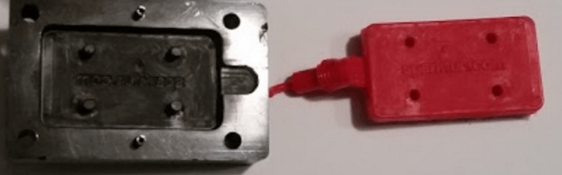
The example shown, the Sparkfun ESP8266 Thing, brings us to an interesting point.
Potting any microwave device with microstrip transmission lines, antennas or distributed filters, etc, is going to stuff up those elements, since they’re designed with the assumption that the surrounding dielectric is air.
Used to see a lot of RF stuff potted with paraffin wax because I guess it’s dielectric constant was well known.
Hot glue works pretty well as a potting compound. Not sure about long-term effects, though, like water absorption or attacking the electronics. Supposedly you can take it off with denatured alcohol, but I don’t know if that applies to a glob surrounding something standing off the board, like a cap or other large component.
Isopropyl alcohol removes hot melt glue from virtually everything. Even takes it off wood, drywall, clothing, glass, metal, whatever. The key to making a good watertight seal with it is using a high temp glue. It flows freely and properly wets into the surface, where low temp/all around type glues only migrate so far into the surface. Water intrusion will happen, and it will ruin everything. I’ve used hot melt glue to hold my lighthouse beacons for my htc vive on drywall and it’s not globbed on, and has held there for months. I sprayed the area with isopropyl while holding to remove it (for sanity) and it frees right up.
I found a different way of dealing with humidity, let it condense, but control the point at which it does and then have a way for the water to escape away from anything it may harm. It seems counter intuitive to let a module breath but if it has a second outer enclosure that is aluminium and then an inner plastic one you can make an enclosure that deals well with pretty extreme weather, but not submersion. Having the breathing ports filter very fine dust helps too, less intrusion of airborne salts during dry and windy periods, because it is the combination that will cause the greatest damage.
Has anyone tried potting a device with an exposed heatsink? The closest I’ve seen are voltage regulators for 50-150cc mopeds, exposed heatsink and automotive style harness connector, with the innards filled with black hard stuff. Since they are often exposed to the elements, it makes sense. And in doing repairs to my 50cc, there are some things I want to add but would like to protect from the same weather.
My thought was to cover the finished board with a soft silicone, but having an exposed heatsink just in case (and as a case to chasis ground) makes a lot of sense. Anyone have some tips?
Yeah, that works well. Bolt all your stuff onto a heatsink, make a little dam/fence around the border of the heatsink using tape, then fill up the dam with epoxy to cover the components.
You can also put stuff in a die-cast aluminium box with high-power devices bolted to the walls and then just fill the box with epoxy. If the box itself hasn’t got enough surface area, you can then bolt a heatsink to its outside.
Be careful that your connectors are mostly-sealed. It’s no good if the epoxy flows through the back of a socket and blocks it.
I read that freezing may work with some epoxy’s, destructive scanning may work for reverse engineering.
I put a BME280 breakout board from Sparkfun in a Stevenson screen outdoors and assumed I was protected. Forgot about condensing humidity. Guess where it condenses? Yep, on the exposed metal pads, shorting things out and killing it.
I encased the next version in two-part epoxy, being careful to leave the BME280 case penetration exposed. It was non-trivial to do right. My hope is that the epoxy I use doesn’t have a high thermal expansion coefficient, and it doesn’t pull away from the sensor chip later, exposing the grid array contacts on the bottom. We’ll see in a few months.
For the Decapers / repair crew: a lot of epoxies break down at 140C.
For the RF guys, if you have to use silicon, definitely use naturally curing as opposed to acidic type, but, also avoid colours, especially black. The black in silicon is often created with the addition of fine carbon particles, and with ageing there seems to be some restructuring, and Eddie currents end up draining your precious RF signals. We saw it on some antenna boxes and it only appears to occur after a period of time, and not on the clear silicon.
NASA link is out of date. Here’s an updated link:https://standards.nasa.gov/standard/nasa/nasa-std-87391
We posted a summary of our waterproofing adventures over the years.
Might be some ideas in there that Hackaday builders would find useful:
https://thecavepearlproject.org/2023/03/17/waterproofing-your-electronics-project/