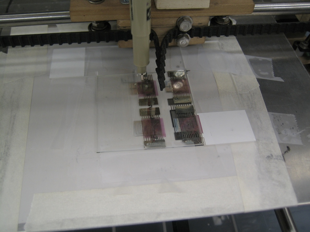
[Mr. Kim] and [John Sarik] made a presentation(pdf) at last weekend’s Botacon conference on how they made organic field-effect transistors (OFETs). A wooden RepRap, the fancifully named Unicorn from Makerbot (or printed from Thingiverse), hacked felt pen, a handful of chemicals, and a couple of pieces of lab equipment were needed to print (plot) out transistors. We were unable to attend the conference, so this is what we inferred from the slides. Silver ink is printed onto a glass slide to form the gate regions, cured and partially masked-off. A layer of CP1 Resin is spin-coated onto the slide to form the dielectric barrier between the gate and the semiconductor, the drain, and source regions. Silver ink is once again used, this time to print out the drain and source regions. The last thing printed is P3HT dissolved in toluene to form the semiconductor region. It would be interesting to see this process modified so that all coatings and curing can be done without removing the slide from the printer.


RepRapped Transitors
@Jeditlan,
good eye. Devlin’s not in yet so I’ve updated it.
Next step: circuit cubes.
Ooooh… DIY ICs sounds awesome!
conductive plastic? how do u do that one?
@kabukicho2001
What do you mean how do you do it? You just make the plastic. Certain kinds of plastic are conductive.
Wow, that is very interesting. If they can increase the density of the transistors enough maybe they could start printing logic controllers for more printing machines….scary stuff.
You caught “transitors” but missed “oganic”. :) I think Hackaday needs an official proofreader (see also “ohmmeter” vs “voltmeter”).
Just out of interest, does anyone else not consider extrusion to be a very exciting way to print?
It seems to me like there are too many hard limits of this method. Resolution and surface smoothness will always be limited and there aren’t really any options for high resolution color printing.
It seems to me like inkjet systems that print solvents into layers of powder are just an outright better technology. If hacking printers is impractical I’m sure that many of the newer half watt blu-ray diodes can perform laser sintering fairly cheaply.
I forsee inkjets and plastic powder where circuits can be laid down between layers. There are even inkjets that print plastic and skip the powder outright. Either way I can’t see this extrusion thing really becoming worthwhile.
Interesting but I looked it up and Wow… $315 for 250mg of P3HT. I sure hope this stuff finds it’s way down to us mere mortal hobbyists at home some day.
@ryan
epson has successfully printed circuit boards using a commercial inkjet printer and conductive ink up to twenty layers thick
that was 6 years ago
Then again, I suppose the amount used per transistor is really really small….
@Christopher Mitchell- idk, i had read ‘organic’, but i had just woken up. it surprises me how Hackaday has posted 2-3 hacks before i wake up, when i sleep like 4 hours.
i would like to print with the Magic Shell ice cream chocolate that hardens when it cools.. and some way to rapidly cool it, without disturbing the liquid. i think LN2 would be more effective than a peltier in larger chocolate models
This technique is great news for hobbyists. I’m so excited about this.
-Jer
Wow, this is great!
For a long time I’ve had this idea to build devices with many of the non heat producing components printed directly to the inside of the enclosure instead of taking up extra real-estate on PCB’s.
This looks promising.
I’ve been dreaming of designing my own ICs since I was 12. It seems like I might actually get to do that someday!
…skynet has humble beginnings…
Where can I find more about the Epson 20-layer printing method? This looks promising, and I think that this community is perfect for its development.
How would YOU do it?
Wow. I guess with a bit of novel spraying and bed heating technology (and heated beds on RepRaps are not uncommon) this might become possible without moving the item off the deposition bed.
There has been work done on fitting inkjet heads to RepRaps too, which might be able to utilise that Epson technology mentioned above. Links welcome.
this could be interesting if a way can be found to make thin enough layers to form memristors.
imagine the possibilities, you could print non volatile memory and semiconductors, resistors etc on the same substrate.
iirc there is a way to make these using silver ions moving through a pair of substrates (think lithium ion cell tech here) and carbon compounds, the resulting resistance versus applied dv/dt resembles a “bow tie” graph.
on a slightly different note, if anyone wants to homebrew resistors a simple way to do this is Durite bicycle repair cement and graphite lubricating powder- my own experiments suggest a highly variable density alterable by ratio of cement versus graphite.
please mail me on mandoline ant cwgsy dont net
(decrud the address :-) )
machines building machines! thats an abomination!
An abomination of coolness !
But yeh, its gonna happen, thats a given.
Oh, and machines already build machines, we arent hammering together ipods or anything like that ..
Reprappery is like .. robots making robots