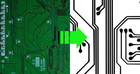
Occasionally when a device breaks, the defect is obvious. Whether it is a blown fuse or a defective capacitor, generally the easy to see stuff is easy to fix. When a problem is more subtle, or when doing some more advanced tasks like adding functionality to a device, greater knowledge about a circuit board is required. While there might be details hidden in lower levels of PCB, often just knowing the mounted components and layout of the outside layers can be enough to create a rough schematic of a device. [Throbscottle] has put together an excellent guide for procedurally breaking down a photo of a board and turning it in to something useful. The guide utilizes some open source image processing software such as the GIMP, Inkscape, and Dia, all of which are widely available. Keep in mind this reverse engineering can be a time consuming process, but will almost definitely reward those patient enough to work through it.
[Thanks to everyone who sent this in!]


Daidified
http://daid.mine.nu/instructabliss/?url=http://www.instructables.com/id/How-to-reverse-engineer-a-schematic-from-a-circuit/
There was a talk at 27C3 (CCC) about reverse engineering PCBs. They are developing software, called dePCB, which is based on the transistor level tool degate -> http://degate.org/.
@d : degate is for reversing integrated circuits (IC’s) from pictures of the die.
Very nice article. Here is a tip though, use morphological operators to trace the track it needs less manual work:
http://en.wikipedia.org/wiki/Erosion_%28morphology%29
It is pretty simple:
1) convert the image to black and white.
2) Use a dilatation operation followed by a erosion operation to connect broken tracks
3) Use the dilatation operator, then make a inverted copy of the image, then subtract the image with the inverted copy. You will get the tracks.
4) Post-process by hand the remaining…
Also, putting the circuit over a light source can help you a lot getting a better picture of the tracks..
Underrated comment !
I was actually most interested in what the flaw turned out to be, not just the happy note that he solved it.
@MrCung @Philip Thanks for the links!
instructables BOOOOOOOO!
Isn’t it much easier to scan the whole pcb using a scanner? I don’t know how well it works with the components still on the pcb though…
This isn’t reverse Engineering – it’s drawing a schematic from a PCB. Drawing a schematic is hardly the same as reverse Engineering especially when it comes to higher frequency, oscillators or circuits that are timing sensitive.
When you reverse Engineer something you fully understand the design including impacts on timing, etc. There are designs out there with specifically designed center planes designed to impact data flow through the board. Some designs even have their own internal tuned coax etched into inner layers.
I did something similar recently, I grinded down the pcb of a phone and took pictures of every layer with a flatbed scanner. Then I used GIMP to trace the stuff I needed, worked great:
http://www.steve-m.de/pictures/pirelli_dpl10/
http://bb.osmocom.org/trac/wiki/PirelliDPL10
Holy carp Philip – that Daid thing is AMAZING!!!!!!!!!!!!!!!!!!!!!!!!!!!!!!!!!!!!!!!!!!
I can actually rear it now! It’s like I’ve re-discovered the internet!
carp=crap & rear=read
(sorry for the spelling – I was a little excited)
I’m using it from now on! WooT!
http://daid.mine.nu/instructabliss/
what about multilayer boards?
can anyone post a link to the pdf ?
There is one article which give out a description of
the general process of pcb reverse engineering.
You can view it at http://www.instructables.com/id/How-to-reverse-engineering-pcb/
multilayer boards are impossible to reverse engineer even manually
“multilayer boards are impossible to reverse engineer even manually”
“atoms can not be split”
“water does not have a prismatic effect, water has rainbows because of the chemicals they put in it”
“the earth is flat”– Le most modern slave of Tzeentch
Comments like this don’t need a report button. A valid login to hackaday should enable users to delete viewing of certain users from feedback comments. Attempting to troll or grief the work of others on collaboration science boards is the same as covering oneself in feces and saying you are wearing the best clothing.
If a person lacks the knowledge; research the topic and formulate a proper question. The war against ignorance is a war any rationally minded person can not remain neutral in.
Awesome fucking comment! you have reaffirmed my faith in humanity. Thank you..