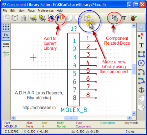
Kicad is a fantastic PCB layout tool. We think creating a part for use with Kicad is in many ways easier than in Eagle, but it never hurts to have a few shortcuts. Here’s a new way to quickly get your parts into the schematic editor. It’s a Python script that generates symbols from an XML input file. You create the XML file with a list of all the pins on your part and the function they will serve. The Python script will then format that as a library file which can be imported by Kicad.
It’s a little bit clunky due to the number of steps in the process. But it is possible to use a CSV file generated in a spreadsheet program to create the XML needed by the script. We’ve used the online component builder ourselves, and appreciate the possibility of mass pin assignments instead of the drop-box for every pin as used by the web interface. One time we were 20 pins into the naming process and accidentally refreshed the page… ugh!
The code is available in their git repository, with a description of the XML format, and a wiki tutorial outlining the component building process. After you give it a try we’d love to hear what you think in the comments.


Hi.
Great tweak, I have used Kicad for several years, I used several Orcad since MSDOS versions and Protel, but now I’m pretty happy with Kicad.
Ditto on that! ;-) I’ve been using OrCad since DOS version 4 (when I believe there was no layout tool), and have tried to learn Eagle, but KiCad is much more similar to OrCad… so it’s my preferred open source choice!
Great to know that you prefer kicad too, I will begin teaching mi new comrades how to use kicad.
I bet this is also possible with Eagle 6, which uses XML “code” in its files. With just a small amount of scripting.
KiCAD is great! Thanks for sharing.
maybe off-topic a bit here but did you tried expressPCB and expressSCH? both are free,unlimited and pretty powerful tools. Creating a part of any shape and number of pins is a breeze in this.
Try it out,see for yourselves.
ExpressPCB does not produce gerber files, and thus locks your design to a specific manufacturer.
I use it to make my own stuff,so that’s not a problem. If you do not intend to have them made by someone else,it’s the right stuff.
Ctrl+p,miror the pdf and you’re set.
That’s not what I heard. Maybe you should actually make just 1 PCB before giving sage advice on which program to use…Eagle and KiCad are great for the hobbyist and the professional. If you are making your own photo etch boards then PCB express might be a good option, but that isn’t very professional.
Yeah, Eagle’s great unless you want to make a mounting hole bigger than .51″, then you can’t. What a stupid-ass program.
Wow that’s a pretty large “mounting” hole. A hole that large will not be drilled by a 1/2″ drill bit though… they will use a small bit and route it out. Why not just define is as part of the board outline and they will route it. If you want it plated through that’s easy enough as well, just fill around the routed hole with copper and sprinkle some notes on your fab drawing to make sure the board house doesn’t miss it.
You can call it names all you want though.. I curse at Eagle when trying to drag a section of circuitry, which takes an unusually high amount of clicks and/or button presses to do what most other programs do by just highlighting and dragging it over the intuitive way.
Hell, I even curse at OrCAD sometimes… but it’s usually operator error. I’m reminded that I’m human from time to time by the mistakes I make. The trick is to minimize the errors by running through developed checklists to keep your design in order. Develop a process that works and stick with it, refining it when necessary. That’s how the professionals do it ;-)
Every other program lets you just make big holes. Absolutely no reason for small limit. They also limit the pad diameter to .51″ as well, which is even more stupid. Every board house I have used has accepted larger drill sizes automatically (I use gEDA). Their software automatically converts it to a routed edge if that’s how they do it.
Oh sure, there’s an overcomplicated workaround that relies on fab notes — oops, there goes the cheap no-touch services. Eagle is a blight.
Yay! KiCAD!
KiCAD is great. But the libraries are inscrutable, you basically have to make your own. And then its hard to manage them.
Fix this problem nerd legion, for I am lazy, I command thee.
Will someone please help out someone who’s relatively new to PCD design? I’ve used KiCAD to design one board and send it off for manufacturing.
What is the benefit of this process? Is this XML schema a recognized industry standard? Can you get XML part files from manufacturers? I don’t see the benefit of manually creating an XML file, using a tool to convert that XML file to a KiCAD .lib file, and then importing that lib into KiCAD, when I could just create the part in KiCAD to begin with. I’m missing something here.
Ad Phils question: for parts with a large number of pins it is sometimes easier to copy&paste the pinnumbers/-names, drop them into a file and autogenerate the symbol. (A spreadsheet app in between may help in formating and organizing the data copied from the datasheet)
You can also get a gps add-on from dual and it has built in microphone and much better speaker