For this year’s 7400 logic competition, [Nick] decided to build an FPGA out of logic chips (Internet Archive cached version).
Perhaps a short explanation is in order to fully appreciate [Nick]’s work. The basic component of an FPGA is a slice, or cell, that performs boolean operations on its input and sends the result on its output. The core of these slices is a lookup table – basically a truth table that stores the result of every possible input combination.
One very easy way to implement a lookup table is to use a RAM or EEPROM chip. By tying the address lines of an EEPROM to the input and the data lines to the output, it’s possible to create a single slice of an FPGA very easily.
Unfortunately for [Nick], 74-series memories have long been out of production. There is another option open, though: shift registers. A shift register is basically an 8-bit memory chip with parallel inputs, so combining a shift register with an 8-input multiplexer is a very simple way to implement a 3-input, 1-output FPGA slice.
After figuring out how to tie these slices to bus lines, [Nick] needed a way to program them. Verilog or VHDL would border on insanity, so he wrote his own hardware description language. It’s certainly not as powerful or capable as the mainstream solutions to programming an FPGA, but it’s more than enough.
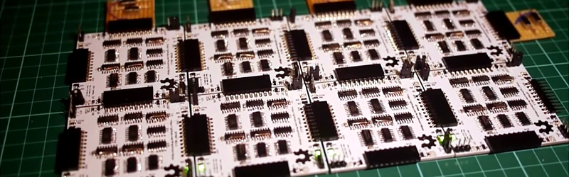
In the video after the break, you can see [Nick]’s overview of his very large 8-slice FPGA while he runs a combination lock and PWM program. All the code, schematics, and board layout are up on [Nick]’s git if you’d like to build your own.


Mother of god.
you have got to be kidding me :-|
Just WOW…
Take something that would most easily be done with a couple of logic chips, but do it with an FPGA, then build the FPGA out of logic chips…
Then if you make a lot of these, you can again combine them to make one of these, and again and again!
Fractal computing!
What about implementing discrete-logic FPGA into normal FPGA? :)
A virtual Pc environment within a Pc.
A virtual 3D engine within a 3D engine.
A virtual file within a file.
A virtual c64 within a AVR.
A virtual python environment within python.
A virtual Fpga within an Fpga.
when??
Error Div / zero
From his blog: “Pointless, given that it’s a fraction of the capability of a moderately priced FPGA or CPLD chip? Probably. Cool? Most definitely.”
+100!!!
Beautifully executed as well.
Too wild! The pointlessness of the thing makes it thousands of times cooler.
And thanks for the brief, “how fpga works” paragraph.
How I hate these creative talented types who can actually make cool things.
Excellent build.
The circle of life.
Holy f*cking shit. Awesome build, but… A lot of wasted lifetime.
Pssh, whatever. I’ll bet he gets all the (s)LUTs
Absolutely incredible…friggin’ awesome work man
Instead of VLSI (Very Large Scale Integration, also the name of one of the first companies to make VLSI chips) this is VLSD Very Large Scale De-integration.
CPLD’s come from FPGA manufacturers…
logic chips come from old devices…
now we can MAKE A FPGA!!!! sweeet.
also… incompatible FPGA on your bench? make a compatible one inside :)
Wait… the PWM program counts, and when it matches, and ONLY when it matches it turns the light on? Am I the only one who sees a flaw with this approach?
If the counter is 0-7 (i.e. 3-bits), no matter what, the duty cycle is going to be .125 (12.5% brightness) — the brightness won’t change.
I think maybe he explained it wrong, or I heard him wrong.
The idea for PWM is to vary the duty cycle — i.e. if the value is 4, then 0-3 should be on, and 4-7 should be off — giving about 50% brightness, versus 0, would be 0% brightness (0-7 would be off), or 1 would be 12.5% brightness (0 = on, 1-7 = off), etc…
I used to be recommended this web site by way of my cousin. I am not
positive whether this publish is written by means of
him as nobody else know such targeted about my difficulty.
You’re wonderful! Thanks!