The Design And Fabrication Of A Digital Clock

boarddesign

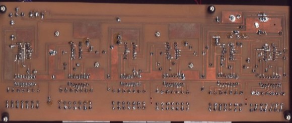
This clock is the first thing that [Kevin] ever made, way back before the Arduinofication of making, and long before the open hardware community exploded, and before the advent of cheap, custom PCBs. It’s an elegant design, with six seven-segment displays, a time base derived from line frequency, controlled entirely by 74-series logic chips. There was only one problem with it: it kinda sucked. Every so often, noise would become a factor and the time would be displayed as 97:30. The project was thrown in the back of the closet, a few revisions were completed, and 13 years later, [Kevin] wanted to fix his first clock.

The redesign used the same 1Hz timebase to control the circuitry, but now the timebase is controlled by a DS3231 RTC with an ATtiny85. The bridge rectifier was thrown out in favor of a much simpler 7805 regulator, and a new board was designed and sent off to OSHPark. Oh, how times have changed.

With the new circuitry, [Kevin] decided to construct a new case. The beautiful Hammond-esque enclosure was replaced with the latest and greatest of DIY case material – laser cut acrylic. Before, [Kevin] would put a jumper on the 1Hz timebase derived from the line frequency to set the clock – a task that makes plugging a clock in exactly at midnight a much simpler solution. Now, the clock has buttons to set the hours and minutes. Much improved, but still an amazing look at how far DIY electronics have come in a little over a decade.


Duo Basic: An All-Logic Chip Educational Computer

DUO

Way back before the days of microcomputers, a few very lucky students first got their hands wet with microcomputer trainers. These simple devices used common logic chips, lights, and switches to perform calculations; basically, a very small and simple computer. [Jack] has just released his DUO Basic 8-bit educational computer, a computer designed entirely around logic chips just as was done in the olden days.

The entire computer except for a single EEPROM giving the computer 256 bytes of ROM, three registers, and two instructions (condition jmp and add). This allows for simple programs to be written just by flipping switches and hitting buttons – it doesn’t get much more ‘bare metal’ than that.

[Jack] has an online assembler and emulator for the DUO Basic along with a few example assembly programs. Of course, all the schematics and block diagrams are available on his site, along with a nice introductory video, shown below.

Continue reading “Duo Basic: An All-Logic Chip Educational Computer”

O Christmas Tree Of Digital Logic

tree

[Chris] over at PyroElectro is getting into the swing of the holidays with a LED Christmas tree build. Unlike the other electrical Christmas trees we’ve seen this holiday season, [Chris] designed his tree entirely with digital logic – no microcontrollers included.

The tree [Chris] constructed on a piece of perf board is a beautiful spiral arrangement of 64 green LEDs.While we’re sure getting all the LEDs soldered to the right height, [Chris] makes it look so easy to create 3D structures with circuits.

The LEDs are driven with a set of eight shift registers, themselves clocked by either a predictable 555 timer chip or a pseudo-random pattern generated with a circuit built from a few hex inverters. By setting the tree to the sequential mode, a pair of lights travel slowly down the spiral of the Christmas tree. If set to random mode, an random number of LEDs light up and walk down the array of LEDs.

Continue reading “O Christmas Tree Of Digital Logic”

Discrete FPGA Will Probably Win The 7400 Logic Competition

For this year’s 7400 logic competition, [Nick] decided to build an FPGA out of logic chips (Internet Archive cached version).

Perhaps a short explanation is in order to fully appreciate [Nick]’s work. The basic component of an FPGA is a slice, or cell, that performs boolean operations on its input and sends the result on its output. The core of these slices is a lookup table – basically a truth table that stores the result of every possible input combination.

One very easy way to implement a lookup table is to use a RAM or EEPROM chip. By tying the address lines of an EEPROM to the input and the data lines to the output, it’s possible to create a single slice of an FPGA very easily.

Unfortunately for [Nick], 74-series memories have long been out of production. There is another option open, though: shift registers. A shift register is basically an 8-bit memory chip with parallel inputs, so combining a shift register with an 8-input multiplexer is a very simple way to implement a 3-input, 1-output FPGA slice.

After figuring out how to tie these slices to bus lines, [Nick] needed a way to program them. Verilog or VHDL would border on insanity, so he wrote his own hardware description language. It’s certainly not as powerful or capable as the mainstream solutions to programming an FPGA, but it’s more than enough.

In the video after the break, you can see [Nick]’s overview of his very large 8-slice FPGA while he runs a combination lock and PWM program. All the code, schematics, and board layout are up on [Nick]’s git if you’d like to build your own.
Continue reading “Discrete FPGA Will Probably Win The 7400 Logic Competition”

Homebrew FPGAs

Homebrew CPUs made out of logic chips are nothing new, but a homebrew FPGA is another matter entirely. [Joshua] sent in a project he whipped up where he made a single logic cell FPGA.

Despite how complicated and intimidating they are in practice, FPGAs are really very simple. They’re made of thousands of logic blocks capable of transmuting into AND, OR, NAND, and XOR logic gates. These logic blocks are all tied together, and with a somewhat complex hardware design language are capable of becoming a CPU, a micocontroller, or even a video card. Basically, programming a microcontroller tells a chip what to do, while programming an FPGA tells the chip what to be.

To build his single logic block FPGA, [Joshua] used a four-bit multiplexer to hard wire a truth table out of a 74HC174 D-type flip-flop. A bit of Arduino code changes the state of the pins connected to the multiplexer allows for any combination of TRUE and FALSE to be calculated for AND, NAND or XOR logic functions.

Yes, it’s only a single logic block for an FPGA, and if this build were expanded to even a few hundred cells it would be gargantuan. Still, there’s no better way to learn the ins and outs of abstract hardware, so we’ll gladly tip our hat to [Joshua] and his homebrew FPGA.

Taking A Look At Decapped ICs

Aside from wanting to play around with nitric acid, [Ben] really didn’t have a reason to decap a few 74xx and 4000-series logic chips. Not that we mind, as he provides a great tutorial at looking at a bare IC that isn’t covered in epoxy and resin.

Most ICs are encased in a hard epoxy shell making it very difficult to look at the circuits within. [Ben] tried to grind this epoxy off with a Dremel tool, but didn’t have much luck until he moved over to a CNC mill to remove 0.040 – 0.050″ of epoxy without breaking the bond wires.

After carving out a nice pocket above the die, [Ben] put a few drops of nitric acid on the chip to dissolve the epoxy coating.  This worked very slowly at room temperature, but after putting the chips on a hot plate the acid was able to reveal the die underneath.

After successfully removing all the epoxy and giving them an acetone bath, [Ben] took his chips over to the microscope and was able to check out the underlying circuit. He doesn’t have any idea what he could do with these decapped logic chips, but the bond wires are still intact so he could still use these chips in a build.

We’d like to see a few decapped MEMS devices, but if you have a suggestion on what [Ben] can do with his decapped chips, drop a note in the comments.

Continue reading “Taking A Look At Decapped ICs”

Retrotechtacular: Simulating Weather Patterns With A Logic Chip Computer

In 1975, [D. L. Slotnick], CS professor at University of Illinois at Urbana-Champaign faced a problem: meteorologists were collecting a lot more data than current weather simulations could handle. [Slotnick]’s solution was to build a faster computer to run these atmosphere circulation simulations. The only problem was the computer needed to be built quickly and cheaply, so that meant using off-the-shelf hardware which in 1975 meant TTL logic chips. [Ivan] found the technical report for this project (a massive PDF, you have been warned), and we’re in awe of the scale of this new computer.

One requirement of this computer was to roughly 100 times the computing ability of the IBM 360/95 at the Goddard Institute for Space Studies devoted to the same atmospheric computation tasks. In addition, the computer needed to be programmable in the “high-level” FORTRAN-like language that was used for this atmospheric research.

The result – not to overlook the amazing amount of work that went into the design of this machine – was a computer built out of 210,000 individual logic chips at a total cost of $2.7 Million dollars, or about $10 Million in 2012 dollars. The power consumption of this computer would be crazy – about 90 kilowatts, or enough to power two dozen American houses.

We couldn’t find much information if this computer was actually built, but all the work is right there in the report, ready for any properly funded agency to build an amazingly powerful computer out of logic chips.