If you’re looking for yet another alternative to etching your own PCBs, then check out this new Instructable on 3D printing test circuits!
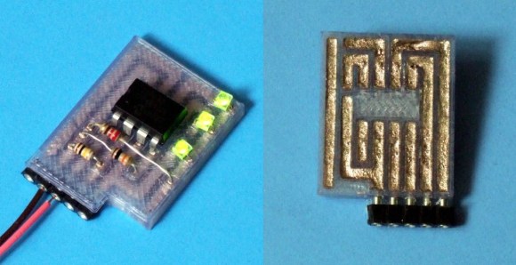
[Mikey] decided to try out this method when he needed a small board prototype. He designed the perfboard to have a standard thickness—only 1/16th thick (~1.6mm)—with thin, recessed channels on one side and through holes on the other. [Mikey’s] circuit board allows you to stuff your components in, hold them down with a piece of tape, and then fill the channels with some kind of conductive material. In this example he’s used a highly conductive paint.
This 3D printed option probably won’t suit all your circuit-building needs, but it could provide an excellent shortcut for your next hack! As always, there’s a video after the break.
Unlike printing your PCBs on a regular inkjet printer, buying a Kickstarter robot PCB printer, etching your own, or modifying your 3D printer to extrude solder, this hack is probably the easiest method you can use—assuming you have the skills to make the 3D model and have access to a 3D printer…
[Thanks Barry!]


I wonder if you could pour in some fields metal to do the filling with a better conductivity. might need a different plastic.
With a little bit of effort this could be easily used to print out new PCBs for more 3D printers. Just use Gallium or Fields Metal for the traces instead. You can then print a layer on top of that to protect it. This could potentially lead to cheaper PCB manufacturing in small batches. Say a poor man’s 3D printer?
I’d avoid gallium. you very well could have aluminum in a part which would get utterly destroyed by the gallium.
Isn’t it also rare-ish, expensive, and poisonous?
Not only that but isn’t the melting point low enough for it to melt in your hand?
Bearing in mind the old melting-teaspoon trick (those Victorians and their wacky heavy-metal antics!), I’d guess it’s below tea temperature but above hand temperature. Unless you kept the spoons chilled beforehand, or something.
To me, the only way I’d think it was a good idea to trick people into drinking Gallium would be after the severe brain damage caused by drinking Gallium.
I suppose if it’s poisonous, you could always swallow a load of Arsenic to neutralise it into LEDs.
I don’t see any reason to do this apart from pure novelty, or maybe to include a couple of traces to an LED on the inside of some 3D printed toy.
The main problem is how fragile and unreliable conductive paint is, and how high the resistance is.
Basically i’m saying that it will make a really cute conversation piece but it’s not a viable way to make circuit boards, just order the damn things from china or etch them using traditional methods.
small steps towards three dimensional circuits. Imagine adding a third dimension to your pcb designs. integrating them with a functional structure. it may seem silly now, but this WILL be a game changer at some point. think big bro.
They exist already, they’re called multi-layer PCBs…
No. Multi layer PCB’s are simulated 3D circuits :)
Multiple boards connected with SIP headers. See the Audrino and it’s shields. There is your 3d circuit
I suppose the problem is, partly, that circuit diagrams have always been 2D, designers are used to seeing electricity move in 2D. Perhaps an increase in Verilog and the like could help computers make the jump. I wonder if you could invent an analogue version of Verilog / VHDL? Would be interesting to see a description of something like an AM radio to start with.
I like your thinking. You could do all kinds of odd shaped, 3D circuits.
I have two comments to this:
1) It is a beginning, maybe we can develop better techniques, better conductive inks, or other complementary technologies
2) It may be exactly what I need. Like a lot of people here I have the need to make small numbers of prototypes, one offs, etc.
Only problem is I have a early onset arthritis (it is more complicated than that, but lets not worry about the details), and my hands shake. I can control them long enough to solder (provided I take a breaks), but it is painful to do for extended periods. Add in measuring and cutting lengths of wire for protoboards and it can be excruciating.
Because of my disability, I don’t trust myself around caustic chemicals and the precision needed to make PCBs at home. Nor do I have a spare $500-$1500 to drop on a PCB mill at the moment.
But I do have a 3D printer. If this technique proves useful then I can make prototypes and proofs of concept and then, and only then send off for PCBs; hopefully saving me time and money.
For the same reason I am very curious about the silver nano particle inkjet technique described the other day (http://hackaday.com/2013/12/05/instant-inkjet-circuits-with-silver-nanoparticle-ink/)
Take a look at how useful the first steam engine ever made wsa, you can see just how well your comments fit and then maybe reconsider your comment. :)
Depending on how far back in time you want to go, the first steam engine was used to open large temple doors automatically when a ceremonial fire was lit.
Usually when an invention is worth something, it is put to some sort of productive use almost immediately. Conductive inks as PCB traces have been around for decades and they’ve remained a novelty because they’re not really suitable even for prototyping circuits.
After all, we can simulate the circuit before committing it to a board, so it’s really only useful for people who don’t want to learn the tools of the trade.
I disagree with your core premise, but I am no interest in debating that point.
Conductive inks are far from a novelty, as [tekkieneet] pointed out they are silk screened for button contacts. I have seen other uses as well.
Breadboards aren’t super portable, or convenient for putting in enclosures. The point of this is that is combines something new (an easy way to make boards) with something established to provide a new possibility. It wasn’t really practical to do this until the advent of cheap 3D printers.
Now let me head off another complaint: durability. Most (but not all) one off PCBs have the useful life of unrefrigerated eggs. This is faster and cheaper than sending off for small runs of boards, and less time consuming/risky/caustic/toxic than etching boards at home.
And of course, there are other materials coming on line that may be much more useful than traditional conductive inks. Like the silver nano-particles mentioned in an earlier HaD post
I have an old keyboard here that has more or less all of it’s resistors printed onto the pcb in what looks like some form of carbon. No markings, completely matt black blobs, some thick some thin. I have never seen these before or since but the manufacturer obviously thought it to be more cost effective to print them rather than then penny or 2 it would have cost to place real ones.
Not really making a point I just thougtht it was interesting and kinda relevant. I wonder how many other types of component can be made in this way? Perhaps a capacitor buy placing a dielectric between 2 layers of printed resistor??
>consuming/risky/caustic/toxic than etching boards at home.
FYI: A few common use for those “toxic” chemicals you are so afraid of.
IHS Chemical: In Western Europe, ferric chloride is used mostly as a coagulant for sewage treatment and potable water production.
Wiki: Ammonium persulfate is a standard ingredient in western blot gels and hair bleach.
So if your “proto” isn’t durable, you are going to THROW it away at some
point and opt to make a proper PCB anyway, right? So that’s same amount
of etching chemicals PLUS more waste from the “proto”.
The only “toxic” part is the copper compound in the waste to lower lifeforms.
You can easily neutralize it and make it insoluble and harmless.
>Most (but not all) one off PCBs have the useful life of unrefrigerated eggs.
If something is worth building, it is worth building well. I spend my
time designing thing to work correctly, so pretty much the initial
“proto” IS the final product. Most of my PCB (“proto” and one-offs) are
build to last and serves useful purposes.
I have a UPS on a home made PCB that is running 24/7 for 3+ years so
far. I trust it enough to for my VoIP/internet.
I think you are focusing only on one aspect of what I said. Please refer to my description of my arthritis and my hands.
But more to the point, I used to make boards at home, and I know the chemicals involved. So when I say I don’t want to touch them with my condition, I know what I am saying
Even easier recipe: hydrogen peroxide + citric acid + table salt. Everything is safe (I checked 3% solution of hydrogen peroxide works, and it does not burn skin), resulting chemicals – are neutral, more or less (copper citrate? It is not caustic and does not cause stains).
@fhunter Good to know, but if you were addressing me (which I admit isn’t clear) you, like @tekkieneet seem to be missing the other things I said about why making PCBs at home isn’t suitable for me (or people with similar issues). The nature of the materials used was just one factor.
Carbon conductive ink silk screened on top of contacts are often used in
a cheap IR remote control. Sometimes it is also silk screened on top of
solder mask as a substitute for wire jumpers for the single side PCB. It
is only used for circuits where the high resistance is tolerated.
I have seen metal conductive ink used in a few applications. e.g silk
screened onto mylar sheets in keyboards, applied in plastic case as last
ditch EMC fix.
To have any practical use for modern day digital parts that requires
power decoupling, you have to get the resistance down. To get the ink
conductive enough, you pretty much have to silk screened as a thick
layer. The viscosity is going to be the limiting factor for any fine
geometry “printing” you are going to do.
As an alternate to using conductive paint, you could design the traces as a bunch of tubes, then all you’d need it a syringe of mercury…
What? Too stupid/dangerous? Naaah. :)
Murcury filled traces would most likely be illegal.
There’s a reason that mercury based switches went by the way side.
Man, I had this idea a while ago… I need to get a 3D printer…
Get PCB in a rod, a sphere, any 3D shape will accept electronics, INCEPTION!
if that 3d printer could print plastic and metal filaments at the same time the traces in the board could be sandwiched inside, at some crazy angles, etc all in 3d instead of usual layers of 2d trace planes
Maybe adding a ring a bit like the collective pitch on a helicopter’s rotor but upside down. With a “finger” to press down and direct the, say enamelled copper wire, into place as the rest of the project is printed. Maybe a follower head to tack it down as it goes.
Instead of printing expensive ink with high resistance, may be it is time to re-inventing the automated wire wrapping machine that use enameled copper wire!
If there is a future in 3D printing PCBs, perhaps the laser-sintering method will do better, since it can produce solid metal very easily. Of course dealing with 2 different materials, 1 insulator, 1 metal, would be hard. Perhaps you could lay a layer of metal powder, sinter it, blow the dust away, then do the same with plastic powder.
Though in sintering printers the powder is left behind layer by layer to support the print. Difficult… Maybe use a liquid to support the powders on a level. Possibly with some sort of surfactants in there.
1 small step for 3d printed circuits.
All these small steps will soon result in a giant leap soon.
Now this is pretty cool. Perhaps you could paint inside holes for multi layer boards? You complain it’s not as good as an etched PC board? I reply, “yet.”
Soic possible?
One possible solution to get better results would be conductive epoxy ( when i recall right up to 80% silver particles). Rock solid and quite good conductivity.
what about solder printing instead of ink?
http://hackaday.com/2013/11/07/3d-printing-with-metal-at-home/
Solder has a much higher melting point than PLA/ABS so who knows if it would melt the plastic and form bridges when being depositied.
Sounds like a question that needs to be answered. I wish I was equipped to test it.
Wiki on solder:
The following are some of the solder types. It would give you some idea
of temperature range. Sn = Tin, Pb = lead, Ag = Silver, Cu = Copper
Numbers are percentages.
lead Sn62Pb38 183C
lead free Sn95.5Ag4Cu0.5 217C
lead free Sn96.5Ag3.5 221C
There is no reason why you have to deposit molten solder other than
convenience. Solder paste is easily available on ebay. A bake in an
temperature controlled oven is all you need to “reflow” solder and even
solder things!
I got a different idea. Copper wires comes in a spool and much better
conductor than any ink. May a specially mass produced perf board that
are divided into component area and bus out the pads into routing areas.
The “machine” X/Y route copper wires and terminates them onto pads in
the routing area. It covers pad with solder paste when done. After it
cooled off, you can populate the board the usual way.
nylon + solder paste + hot air, bingo!
ABS’s melting point is 105C and PLA is even lower. If you put it in a oven hot enough to melt the solder paste, you’re going to melt the ABS/PLA too.
How about Carbon Nano Tubes? Combined with epoxy it would be viscous when forming, light and strong when dry, durable and conductive. great wiki on it here:
https://en.wikipedia.org/wiki/Carbon_nanotubes
Check out the ‘paper batteries’. (Where your housing becomes your power supply)
I wonder how long before it will be available for individuals to utilize. Game Changer when it does.
Ursus.
https://en.wikipedia.org/wiki/Carbon_nanotubes#Toxicity
“Carbon nano tubes deposit in the alveolar ducts by aligning length wise with the airways; the nano tubes will often combine with metals. [73] The needle-like fiber shape of CNTs is similar to asbestos fibers. This raises the idea that widespread use of carbon nanotubes may lead to pleural mesothelioma, a cancer of the lining of the lungs or peritoneal mesothelioma, a cancer of the lining of the abdomen (both caused by exposure to asbestos). A recently published pilot study supports this prediction.[74] Scientists exposed the mesothelial lining of the body cavity of mice to long multiwalled carbon nanotubes and observed asbestos-like, length-dependent, pathogenic behavior that included inflammation and formation of lesions known as granulomas. Authors of the study conclude:
This is of considerable importance, because research and business communities continue to invest heavily in carbon nanotubes for a wide range of products under the assumption that they are no more hazardous than graphite. Our results suggest the need for further research and great caution before introducing such products into the market if long-term harm is to be avoided.[74]
Although further research is required, the available data suggests that under certain conditions, especially those involving chronic exposure, carbon nanotubes can pose a serious risk to human health.[69][70][72][74]”
So are you trying to say that might not work?
or are you just pointing what is true of the vast majority of materials used in manufacturing (including sawdust)?
Your comment did make me notice something i hadn’t before, however.
That is, the section you quoted above was about the only negatives present within that rather large wiki page regarding the properties and potential uses of carbon nano structures.
thasnks,
ursus
Also possible are alloys using indium and other metals.
One that has been studied is as little as 8% indium but as it just fills up grain boundaries you don’t need as much of it.
Also useful are bismuth/indium/tin/zinc alloys as no lead is present, yet the MP is still less than 120C.
How about taking a piece of board, putting on a swath of double-sided sticky tape, then placing bare wires and components on it, then dab all the junctions with solder. Presto, quick circuitmaking without a 3000+ bucks 3D printer and 50 bucks per microliter conductive paint.. And it’ll still be feeble, although a swipe with some epoxy should fix that.
Lovely strawman you have there, pleased to meet it ;)
I suggest you revisit the prices of 3D printers, they have really come down in price. But you are right if your point is that it would be foolish to buy a 3D printer just to make circuit boards. However if you already own one, well that changes the math.
And yes conductive ink is expensive, but an ounce goes a long way. I use a bare conductive pen for the occasional prototype and interactive cards and I am just now running out.
I have a hard time grasping the negativity to this post. It is just one more tool out there. Maybe it will be nothing more than a novelty and of limited use, or perhaps it is the beginning of something bigger. No matter what it is a cool hack, and every hack we are exposed to helps inspire something else.