

The Hackaday writers and readers are currently working hand-in-hand on an offline password keeper, the mooltipass (click to see the project description).
Next in our Developed on Hackaday series, we present the first version of our schematics. There’s already been a lot of discussions going on in our dedicated Google group, mainly about the project’s basic functionality. Because our firmware developers wanted to get to work, we decided to send the first version of our hardware into production a few days ago. Before going through the schematics, let’s review the required list of the mooltipass’s core components:
- an easily-readable screen
- a read-protected smart-card
- large flash memory to store the encrypted passwords
- an Arduino-compatible microcontroller with USB connectivity
We’ve been drowning in component suggestions from motivated hobbyists, so we figured we’d make the mooltipass v1 as simple as possible and then move from there. Given this device is developed on Hackaday, we also wanted future users to modify it, building completely new projects based around these main components. Keep reading for our schematics…
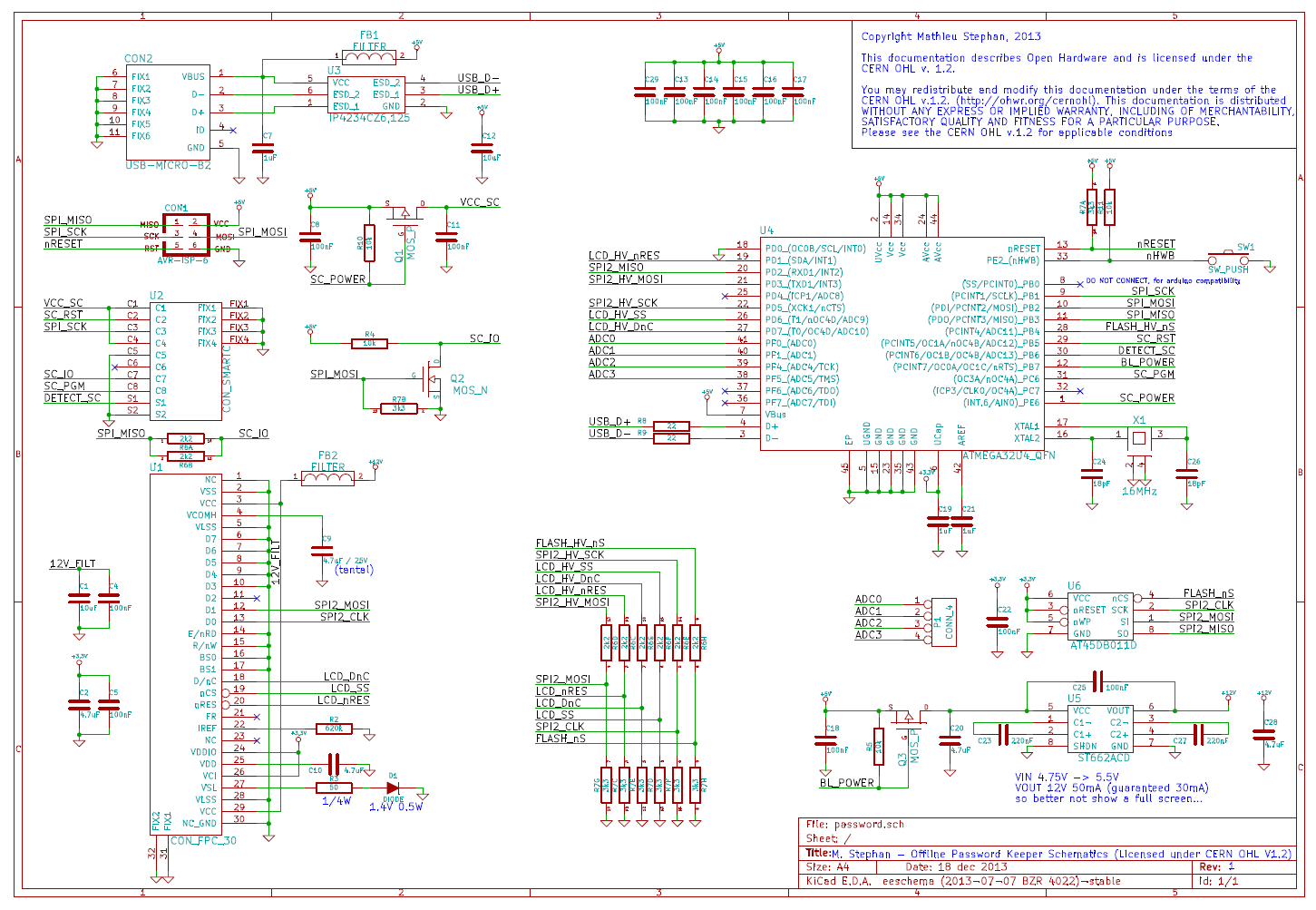
For the core of the platform, we opted for the ATmega32U4 from Atmel. It is the same microcontroller used in the Arduino Leonardo, allowing us to use the numerous libraries that have been developed for it. In the final schematics, we’ll add an expansion connector so users may connect additional peripherals (we may switch to a 4 layers PCB at this point). The microcontroller’s USB lines are protected from ESD by the IP4234CZ6 from NXP.
For encrypted passwords storage, we found the cheap 1Mbit AT45DB011D FLASH which also has 2/4/16Mbits pin compatible versions. If our beta testers find that 1Mbit is not enough, upgrading the mooltipass would be easy. A few readers may already know it, but when picking a flash memory, special attention should be paid to the minimum amount of data that can be erased in the chip. If the flash doesn’t have an internal buffer (like the one we selected does), the microcontroller must read a complete chunk of data, modify the relevant part and resend the modified chunk to the memory. Given the ATmega32U4 only has 2.5KBytes of RAM, this may have been problematic.
Finding a smart-card that could provide the desired security functions wasn’t the problem, but finding a supplier that could send us relatively low quantities (<1M) was. We did, however, find the quite old AT88SC102 from Atmel, a 1024bits read/write protected EEPROM. It can be sourced for less than a dollar and our security assessor didn’t object to this choice. It also uses an odd bus for communications (SPI-like with an open drain data line), which is why we used the N-Mosfet Q2.
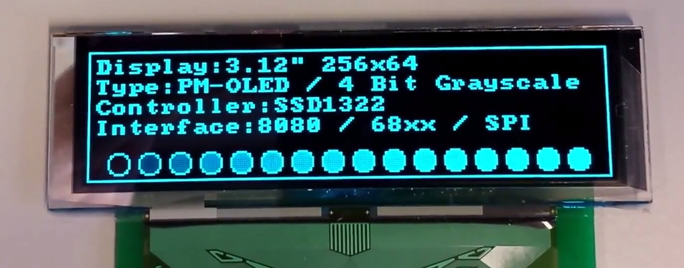
A hot-topic in the Google group was the display choice. Although opinions were varied, we agreed on the core constraint that the chosen display should be at least 2.8″ and read easily under bright light. High resolution and RGB wasn’t necessarily required, so as a first try we’ve opted for the OLED display shown in the picture above (image taken from YouTube). After several weeks of looking for viable alternative OLED screens without any success, we’re currently considering making another mooltipass version with an IPS LCD. Moreover, the current unusual 3.12″ diagonal means we’ll need to have a custom-made resistive touch panel: the quotes we received for the capacitive ones were too expensive.
These components choices made the voltages electronics fairly simple. The whole solution is powered by the ~5V coming from the USB, and the ~3.3V required by both the flash and the display is provided by the ATmega32U4 internal LDO regulator (~55mA @ 3.0 to 3.6V). The +12V also needed by the display is generated by a $1 regulated charge pump DC-DC converter. If we had to use a conventional step-up, the component count (and cost) would be much higher. Notice that we put a P-MOSFET in series with the latter as the output voltage when the DC-DC is not working is not 0V but VCC (here +5V). We also used another P-MOSFET to switch the power supply going to the smart card.
We used two resistor networks R6&R7 (easier to solder) as voltage dividers to transform our 5V signals to 3.3V. Fortunately, the ATmega32U4 can receive LVTTL signals, so we don’t need level shifters to get the data coming from the 3.3v-powered flash memory.
That wraps up the mooltipass schematics overview. If you have any suggestions, you can contact the team in our dedicated Google group. Of course we’d love to hear general comments, please share them below.


Anyone know where to source such an OLED display? I’d like to have one just to toy around with, but can’t turn up any that are this big in the usual places (eBay, parts suppliers).
I still have yet to use Alibaba or AliExpress… is this the way to go?
I actually forgot to mention that the one shown above will be directly provided by the manufacturer (Densitron)
Even though I previously said “I would hate to eBay source items” something like : http://www.ebay.com/itm/3-2-inch-TFT-LCD-module-Display-with-touch-panel-SD-card-240×320-than-128×64-lcd-/200908823757?pt=LH_DefaultDomain_0&hash=item2ec7195ccd isn’t the worst idea ever (Note: It appears to need more IO than the 32u4 possesses)
thank you! I had once found this screen but couldn’t find it again. However, it’s a TFT and the resolution is a bit big for what we need :)
http://www.ebay.com/itm/2-4-inch-TFT-LCD-module-Display-touch-panel-SD-card-240×320-than-128×64-lcd-/400373179957?pt=LH_DefaultDomain_0&hash=item5d3819e635 2.4 inch perhaps? Still TFT and it looks like it has the same resolution. I just happen to think those OLED screens are a bit pricy, especially if you have to have a custom resistive touch panel. (Serial ‘shields’ are available for these as well)
You can get it from here: http://www.buydisplay.com/default/oled-display/3-2-inch-oled-display.html
They even have different colors!
I’ve been sourcing them from the mt 3 main suppliers, RS, Digikey and Farnell all carry them. Here’s the link for similar displays at Farnell:
http://uk.farnell.com/jsp/search/browse.jsp?N=2031+202990+110199437&Ntk=gensearch&Ntt=oled&Ntx=mode+matchallpartial&No=0&getResults=true
from my 3 main suppliers*
You are aware that the 10 µF capacitor C1 is effectively only 2 µF at 12 V bias? Similiarly, C9 is 1.9 µF and C12 is 5.5 µF.
You are aware that there is a google groups site specifically for this kind of discussion? Idiot.
no name calling. this comment is very informative and relevant.
I agree anonymous Vs. anonymous name calling can drag thing down. However while I would preferred thatYahoo groups or the hackaday forums had been used to create a forum I agree with the implication that discussion of details be kept at the the designated forum/group. First because good information will be scattered about multiple Hackaday articles. Second being the way comments to articles are threaded. When both are combined you will be left with a piss poor archive of the progression of the project. I understand there will be those who will balk at any requirement to register to register to follow or contribute to the project but I’m not sure why they should be allowed to dictate how others manage a project. Respectfully that’s my opinion.
Hey Thomas,
Thanks for noticing it! We had forgotten to look at the detailed specs… we’ll switch to another cap for the next revisions.
Hello, can you explain why this is the case? For those of us who are not so well versed in the detail?
Thank you.
In short, the actual capacitance of a capacitor varies with the applied dc voltage… the higher the voltage, the lower the capacitance
Can you go into more detail about why this is happening? I thought that the capacitors would just be their printed values unless in extreme heat conditions or if they were over their maximum voltage.
The capacitance of MLCCs depends on many factors such as temperature, dc bias, ac amplitude, age, frequency and the phase of the moon. The most surprising one is DC bias, which means that you can have capacitors that are rated 25 V but only have about 5% of their capacitance at the rated voltage (e.g. CL10A106MA8NRNC). The 10 µF capacitor on the BOM is GRM21BR61C106KE15. It’s not always easy to find detailed datasheets for MLCCs, but Murata is pretty good about it and you actually get the datasheet linked from mouser (digikey only has a generic catalogue that isn’t very useful).
http://psearch.murata.com/capacitor/product/GRM21BR61C106KE15%23.pdf
If you look at the DC bias curve, you’ll see that at a bias of -80% at 12 V, which specifically means that if you the voltage across the capacitor is the sum of a 12 V DC signal and a 0.5 Vrms AC signal of frequency 1 kHz, the measured capacitance is 2 µF.
Thank you Thomas, I was not aware of this effect! I guess this is why it is always important to know your datasheet.
Regards,
-Kevin
Good explanation. I wish you would do a video where you go thru all those diagrams in a datasheet and just explain very detailed what it can tell about a part. Because I’m a bloody beginner and need people like you :D
Only if they are Y5V or other crappy dielectric like this. Good stuff like X7R will only lose a few percent. I don’t see dielectric or even rated voltage stated anywhere, though…
That is not completely true, either. Check out this article from Maxim –
http://www.maximintegrated.com/app-notes/index.mvp/id/5527
It was also published on EDN and I can’t remember where I found the link… The Amp Hour, maybe?
Being that you only have 2.5K of SRAM available total, less after things are running due to the environment, all your graphics etc will need to be generated on the fly or loaded pre-fab from flash with no frame buffer. How graphical are you guys planning on going? With touch, graphics will be integral to the form and function of the device. Its conceivable you could use the on-board dataflash to store graphics, but you will probably need a larger part than 1 mBit if you want any room left for other stuff, especially if you use the grayscale functionality of that display!
Luckily enough we have a frame buffer in the screen controller. Nothing has been said about the graphics we’ll generate yet. We may not need to use all grayscale levels though :)
Shouldn’t be too hard then! Any Idea on a target price for the BOM yet? I suspect the displays have a minimum quantity, coming direct like that… Not to mention the touch panel…
Looks like a cool project! If I wasen’t so busy with work and consulting, I would love to help out! I will be following closely and watch for updates…
Just a word of warning: a four layer board will most definitely double your fab costs. Stay away if you can avoid it!
I hope :). Current BoM price is around $28 without the touch panel ($20 for the oled… that’s why we’re still looking for other screens).
Since seeedstudio started to make 4 layers boards, we found that prices dropped quite a bit. Given the PCB shouldn’t be too big, we hope the price difference won’t be too big. I’m a bit worried about putting too many traces on the ground plane :/
Not sure about this particular controller, but be aware that most small LCD/OLED ctrls I’ve worked with supported WRITES ONLY when the serial/SPI-like interface was used. In order to get full normal R/W access to the embedded frame buffer, you’d have to use the 8-bit 8080 or 6800 parallel interfaces.
With a write-only FB you’ll need some shadowing in internal uC SRAM anyway, or always have to overwrite full bytes (e.g. two 4-bit or eight 1-bit pixels) instead of single-pixel updates.
The drawbacks of parallel i.f. are obvious: requires some 11-12 I/O-pins for the bus vs 3-4 for serial, but on the upside much higher bandwidth for display updates and often-desired R/W access to the external FB.
Looks like you are pipped at the post
Here is one where you point your phone at the screen?
Would this not be a better approach if you can pick up on it?
http://bits.blogs.nytimes.com/2013/12/18/new-clef-plug-in-lets-you-forget-about-your-password/
Where are the Kicad libraries required to open your kicad project filesplease?
The email address box does not come up when I go to comments on Linux Mozilla Seamonkey browser
This project is quite different (not open source, you need to trust your phone…).
You could have used the cache library in the project folder, but I just pushed my library to the github :).
I know its nitpicky, but I really wish more people would attempt to compose their schematics as, well, actual schematics. This terrible style of just plopping down all the parts and then drawing little wires on each pin to merely attach a net name is about as non-schematic as possible.
Ok, done ranting…
That style is acceptable ff the parts in the schematic are drawn to represent their physical form, with the pins laid out in numerical order. But when the parts have been drawn logically (as they are in this schematic) then it only makes sense that the circuit should be actually drawn out, after all what was the point of re-arranging the pins in some logical manner?
“mooltipass” as in what Leeloo called her Multi Pass card in the movie “The Fifth Element”? M’kay…
Yup. My fault.
xD
What does “arduino compatible” mean? Does teensy count? Does arduino due count? Does teensy 3.x count?
The GitHub project suggested showing a QR code as an option. This is potentially insecure as some QR reader implementations send codes to third-party services to decode the QR rather than keeping everything local to a phone/device. On the other hand, there are some integrated bar code and QR readers that could work with this feature.
Yay! Kicad!
Okay, sounds cool. I’ve had such a thing for a while, but it’s composed of attiny2313 & 64KiB i2c EEPROM stuffed with VUSB stack, so time for a change.
I’ll be happy to help you out with a pam module.
Just one little suggestion:
Please, DO NOT make arduino libs a hardcoded dependency for your firmware code – make it just plain C, that you can later wrap into an arduino library or two for the *duino addicts out there.
### Suggestion ###
Why not put buttons under a more square oled like http://hackaday.com/2010/01/27/nanotouch-a-tiny-avr-media-thing/ and drop the touch screen… its too small to use touch properly anyway and id rather have a nicer screen.
we actually sent a survey on this topic in the google group :)
I actually forgot to mention that the one shown above will be directly provided by the manufacturer (Densitron)
With a community developed project like this, I would think it is likely that someone would try to sneak a backdoor into the development of the project. Perhaps someone (or many people) should review all code and hardware to try and spot security weaknesses hidden by community developers? Just an idea. I love the project though and wish I could contribute more at this time!
^ On that note, perhaps a competition to hack the mooltipass later on would help the community discover any security weaknesses. Ok, I will stop posting now :)