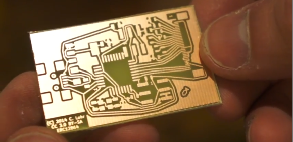
If you’re going to learn something, it only makes sense to learn from a master. [CNLohr] is known around these parts for his fablous PCBs, and he’s finally started to document his entire fabrication process.
[CNLohr] is using a photoetch process, where a mask is created with a laser printer on overhead transparencies. He covers the copper clad boards with a Riston photosensitive mask—available here, and they accept Bitcoin—sent through a laminator, and exposed with the laser printed mask and a UV grow bulb. After the mask has developed, [CNLohr] drops his boards into a ferric chloride bath that eats away the unexposed copper. He then removes the photomask with acetone and cuts the boards with a pair of aircraft snips, and they’re ready to be soldered up with components.
Yes, home PCB etching tutorials are pretty much a solved problem, but [CNLohr]’s work speaks for itself. He’s also the guy who made a microcontroller/Linux/Minecraft thing on a glass microscope slide. Learning from a guy with these skills means you’re learning from one of the best.
Video below, and there’s also a video going over the design of a PCB using KiCAD (!) and TopoR (!!!) available here.


Those traces are making my eyes bleed.
Yep, TopoR.
Cool looking concept for layouts. Thanks!
Now that’s how it is done.
I wonder what happens if you hit cheap parcel tape with a UV light…
hmm, dont have to click an ‘agree to terms of service’ to make a comment yet…
I used to use the following method, about two decades ago to make printed circuit boards, both single sided and double sided versions,
laser printer + paper (no transparencies yet, at that time) + photo resist (positive or negative) + vacuum box with ultra-violet exposure machine + printed circuit on plain paper (positive or negative mask) + sodium hydroxide + ferric chloride crystals (with hot water)
-print the correct circuit board (on paper) and use correct photo resist on the PCB,
-place together the printed circuit (on paper) paper + cleaned PCB (with photo resist)
– turn on the vacuum (box),
-turn on the UV light on for ~ 5 minutes on the correct side (top or bottom or both, check alignment if using both sides),
-the mask will be formed, use sodium hydroxide to wash off the undeveloped mask,
-touch up broken tracks with a permanent marker, use single motion to draw, not multiple motion,
-etch in ferric chloride solution, hot water will speed up the etching process,
-clean the etched circuit board and drill the holes if using through plate components,
-finish…
A couple people have recommended using regular paper. This Riston stuff is SOMETHING ELSE. It is far better than anything else I’ve dinked with. What is the purpose of the vacuum box? I always wanted one, but have yet to find a real need.
Back in the mid-90’s as an undergrad I would use a similar process developed by my boss. I’d:
* Print from Protel for MSDOS to a HP Laserjet BUT I’d cut out A4 sheets off a roll of that semitransparent (milky) drafting paper instead of regular paper.
* Expose the orange negative film with the laser print. They’d be squashed firmly together between two A3 sheets of glass and large paper clips holding it all together.
* Expose in a large home brew UV box
* Develop the orange film with some kind of chemical by gently wiping it with a cotton ball.
* Expose precoated PCBs again in the glass sandwich with the orange negative..
* Wash the exposed PCBs with acetone to get the unhardended blue gunk off.
* Etch in a bath of some solution I forget.
I could do double sided boards quite easily with excellent registration. Hand drilled the vias with a Dremel like drill on a pedistal.
Now, if Protel of the day could have printed the PCB with black and white inverted the orange film step probably could have been eliminated.
We made a big arsed 386ex double sided PCB prototype this way, amongst others.
Don’t forget to wipe clean with alcohol and varnish the boards while the copper is still shiny.
Couldn’t make photoresist film work. You need to be able to SEE to get the film applied, inspect it for and remove major inclusions (a big pet hair or two always seemed to get in there), reapply the film, run it through the laminator, register and affix the mask, and so on. Working as fast as I could with various dim light sources (red incandescent, LED, fluorescent, tried them all) and keeping the film covered at all possible times, I either found the film exposed all over due to excess light, or unusable because the light was so low I simply couldn’t see where I’d made a major mistake. After a dozen failed attempts I gave up. Maybe my film was too sensitive, or whatever, but it’s definitely not as easy as I’d been led to believe.
I had a bear of a time with this stuff before I found out how to do a wet application. It was terrible. There would be dust, bubbles, you name it, and it would ruin a trace. Now, my adherence is almost perfect. The LED work light is really a godsend. I tried using it with an incandescent, and it did have exposure problems.
Additionally, I do occasionally have under or overexposure issues, but they are very rare now. It probably took 30 prints with this new process before I started to really get the hang of it, but every time I do it, it’s faster and faster.
P.S. Did you use Riston?
Unsure of the manufacturer/product now, was purchased from Ebay, all this happened many years ago. [James] below is claiming far better resistance to accidental exposure with Ebay films than either of us saw, claiming normal room lighting is ok, and that’s what I was expecting going into this. But working at night with the room lit by a single shaded 23W 2,700K CFL, the film was totally exposed in under 10 minutes! The wet application sounds interesting, and perhaps I will experiment again someday – with a different film, and NOT when I’m in a hurry to complete something. ;)
Not sure if this is useful, but CFL like all fluorescents has a surprising amount of UV leakage. In a lab where I used to work, we exposed photoresist boards just by putting them under fluorescent ceiling lights. In prep we used a “red bulb” (an incandescent painted red) to avoid exposure, and I knew a guy who swore by a home-brew panel of deep red LEDs.
Dry film, at least any that you can buy on ebay is simply not very sensitive to normal every day household lighting. Obviously don’t work in front of a window, but I’ve never had an over exposure problem just working under normal lighting conditions. You’d have to be spending a couple hours, probably quite a bit longer, trying to affix the film before you had that problem!
I don’t use a laminator, I just use a clothes iron, I find it easier (especially with small boards I do, up to about 7x10cm). Clean the board, just like you would for toner transfer. Cut a piece of film, a bit larger than the board. Two bits of sticky tape one either side of corner of film, pull apart and one of the protective films will remove (the inside of curl). With a cool pcb (15-25 degrees C) touch the film at one corner, and use your finger to spread it down evenly, your body heat will give it enough to stick lightly. If you got a bubble, prick it with a knife tip, smooth it down.
Take the clothes iron, on a COOL setting, probably only a couple of clicks above the lowest it can go, sit the iron on top, for perhaps 20-30 seconds. Then run the iron over the whole board with typical clothes-ironing-pressure, especially the edges, use the iron tip on any areas where you pricked bubbles to make sure you “buff it out”. A COOL iron is the key I find, too hot and it blisters (but too cool and it doesn’t stick, once you get some practice you’ll have marked on your iron where to set it).
Print artwork on good quality fairly heavy tracing paper (I use 110gsm). Expose for probably a shorter time than you think you need (I use 53 seconds with my fairly strong UV led array, sunlight about the same), longer exposures give darker traces, but if your artwork isn’t highly UV opaque you will have a harder time developing.
Develop in 30 grams per litre of sodium carbonate, cold. Takes 2-3 minutes usually. Rub gently between your fingers once it starts going gooey, it will rapidly clean up. If you have to do more than that to get it clean (electric toothbrush for example), try a shorter exposure next time. Important! Rinse in clean water, flowing preferably, rubbing with fingers, you want to stop the developing and get rid of residues as much as you can.
I then give it a 5 minute blast of UV to further solidify and harden the traces.
Touch up any iffy bits with a resist pen (eh, a bit of dust on the artwork,didn’t quite get enough heat… you’re a hobbyist, touch up is inevitable), note due to residues you may have to clean the tip of your pen on some paper now and then. Etch, rinse, and then drop in about 60g/L NaCL until the resist is removed.
Re-exposing after development – why do I never do this? It’s obvious. I even do this for my UV solder mask, but for some reason it didn’t click for the etch resist.
I suppose it might not necessarily make it more resistant to the etchant (as opposed to the developer), but seems like a sensible thing to do.
Nice to see a post about etching that doesn’t think the only option is toner transfer.
For anyone starting out with photo etch, I’d recommend a presensitised board. It might be a bit more expensive than laminating or spraying the resist on, but saves you one step.
@CNLohr – Vacuum boxes ensure the transparency is evenly and securely pressed against the PCB during exposure. If you’re not getting any light leaking under then maybe you don’t need it. Hack tip – try a Ziplock vacuum food bag for a cheap alternative.
What a messy Layout. This is the second one of that type I have seen in the last weeks. Are you guys mad?
Topological routing…. Not gridbased Not for the anal-retentive. Generally reduces total trace length and number of vias… As a side benefit, it also pisses people off.
As a side note, totally not recommended for an RF or high speed circuits.
Breathing acetone fumes is not healthiest way to make those PCB’s :) You definitely need a good ventilation. FeCl3 is really most nasty thing than sodium persulfate.
The most interesting thing i’ve seen that, how you make that footprint in Kicad? What the most effective way is to make footprints in a fast way? Wich conception you’re using? E.g. First set size of grid. Then set pad size settings and than placing them etc.
Positiv 20 (Kontakt Chemie) did well for me 30 years ago.
I tried acquiring this originally before giving up and going for Riston. Is Positiv still available?
This is a very interesting process. Thanks for sharing.
Is there an alternative to 3 in 1 oil?. Could i just use cooking oil instead?
Please, can you tell me that, how can i print the negative layout for PCB febrication. as when we expose the Layout on the Board, the image that we obtained is opposite