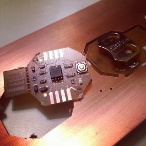
Last super bowl Sunday, instead of checking the game, [Mattw] decided to extend a design and make a PCB of a trinket clone. [Mattw] altered a trinket clone design by [Morgan Penfield Redfield] to shrink it down, perforated the USB connector to allow for easy removal and put most of the parts on a single layer.
After finalizing the design, [Mattw] put it into the LPKF Protolaser S that Seattle’s Metrix Create Space has. For those of you who don’t know, the LPKF protolaser uses a laser to directly ablate off the copper from the boards. This makes prototyping much faster without the need for a lot of nasty chemicals.
About six minutes in the Protolaser, some component placement by hand followed by a run through their reflow oven and [Mattw] had three boards ready to be tested. All told, about 4 hours from start to finish.
The end circuit looks great and the LPKF protolaser gives us a case of serious tool envy. If you’re like us and don’t have access to the fancy laser you might try our hand at this high-resolutino photo-etch process.
[via reddit]


Why exactly was it necessary to run this through a reflow oven? It says that it took an hour to “paste and place” four boards, then there was the reflow. It should take under 5 minutes to populate one of these boards by hand with some small solder… And he had to use a soldering iron anyway (for the vias). Am I missing something here?
Where ablated copper ends up?
I was wondering that too. The video shows an exhaust hood so it must all end up coating the cars in the parking lot. Hmm, wonder if you could reclaim the copper for deposition at a later time. Neat looking toy though. Kind of interesting that it does diagonal scan lines.
“Where ablated copper ends up?”
Laser ablation sublimates/evaporates (plasma state) so it ends up in the air and potentially coating anything that ‘it’ comes in contact with. That machine has a HEPA and active carbon filter on the air compressor so that is air intake cleaning only. There is a 3 bar vacuum takeoff from the compressor that pulls air from the case of the main laser unit to the ‘vacuum cleaner’ (LPKF words, not mine). This is just an standard industrial vacuum-style air box. In lab environments you vent that box to the outside world. No active filtering is going to remove airborne metal particles of the size produced during an ablation process.
That said, yes, there is causal effect/relationships to airborne metal (including copper) particles and small-cell lung cancer, you can find published papers from various schools, research centers and the CDC, DHS, etc.. (even reports from the BLM!) …
But if you have a 3d printer on your desk and wonder if the great hot corn smell (pla) or that sick chemical smell (abs) is going to be toxic to you in 20-30 years… well, time will tell I guess… Personally I assume breathing 1 to 2 hours of toxins coming out of the tailpipe in front of me everyday during my commute will prove just as toxic long term….
IHMO: Any device that melts, burns, ablates, cuts, etc… any material should not really be next to you for 8 hours a day while in operation if short and long-term health safety is not handled with positive airflow, protective clothing, filtration, … , but I think that should just be common sense….
Not sure if the fumes from the laser is worse for you than the “nasty” chemicals which can be neutralized and disposed of responsibly…
I just dump them down the drain, who cares.
That routing looks ugly to me. I wonder if it’s auto-routed.
If it functions does it matter?
According to the article “I really enjoy the zen of routing single sided boards”. So, why settle for unnecessary ugliness ?
I guess it is the journey and not so much of the destination. :P
Wish people would pay attention to *proper* decoupling their chips i.e. minimize the inductance (i.e. short fat track and/or fills/planes) to decoupling caps. I am talking about the 2 ceramic caps at the upper left corner. They are not decorations that you sprinkle onto a PCB.
A person in Seattle was NOT watching the SuperBowl????
Run him out of town! B^)
P.S. I probably would’ve done the same thing if I could…
So it was Proof of Concept, or does it do anything? (no video of flashing LED’s or whatever waah-waah-waah) B^)
I’ve got a LPKF mill for milling PCBs.
It’s a small german company, about 15km from were I work (Hanover, Germany)
If you’re going to ablate the copper, why not try to minimize the amount of copper removal ? I’d use fatter traces, and a ground pour.
“The hybrid cutting head of the LPKF ProtoLaser allows for alternating
use of the mechanical milling tool and the laser beam. The laser beam
creates the critical fine structures, and the mechanical milling bit
removes large copper areas, drills holes, or routes the contour of the
board.”
Still, even with the milling tool it would be better to leave as much copper on the board as possible, to minimize wear on the bit.
Has anyone got a link to more info on that Protolaser S? All I’ve managed to find is that it’s an IR laser and that (no surprise) it’s not cheap at about $140k.
I’m guessing that it’s a completely different animal to the more common CO2 laser (also IR) which reflects off copper and would make a mess of the FR4 underneath. Shorter wavelength and ultrashort pulse maybe?
just wondering what would happen if i’d stick an adhesive plastic foil to the pcb, and use the laser to remove the plastic where it needs to be etched. and then a quick bath in those nasty chemicals. i think it’d require a lot less horsepower to burn it off.
theoretically it could be done with those blinding 1-2W blue laser pointers. or with a laser diode scavenged from a dvd burner.
I seem to remember an old HaD article about a guy using black automotive paint as the resist. He then used a laser to “burn off” the paint in the non trace areas. Similar idea. (Search in HaD doesn’t work for me so I can’t look it up.)
You mean this?
http://hackaday.com/2013/05/11/laser-cutter-helps-make-dual-sided-pcbs/
You need a more powerful laser for that. 1-2W won’t cut it. The reason is the huge heatsink below the foil, the copper!
Beautiful smooth design. I have trinket clone to. Is compatible with Digispark but smaller and with RGB led. https://www.tindie.com/products/bobricius/picoduino/
you guys misspelled [morgan redfield]
Thanks, fixed