Making PCBs at home is a great means to get your prototype up and running without having to wait weeks for a professionally made board. Regardless if these prototype boards are milled or etched, they are easily identified as ‘home brew’ due to their ‘unfinished’ appearance. [HomeDIY&Stuff] has put together a little how-to on the process for making DIY PCBs look a little closer to a professionally manufactured board.
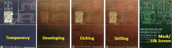
The process starts out with designing the board in a PCB program. There are a lot of these programs available. Eagle is a popular choice and has a free version available. Once the layout it finalized, the design is printed out on a transparent sheet of plastic. A blank copper-clad PCB board that already has a UV sensitive coating applied are available for purchase and is what is used in this example. The transparency is placed over the PCB blank and then exposed to UV light. The coating on the PCB cures where ever the UV light passes through the open areas of the transparency.
Once the transparency is removed, there is a noticeable difference in coating color where it has cured. This board is now placed in a developer solution that removes the un-cured UV sensitive coating. A Ferric Chloride acid bath then etches away at the now-exposed copper. The cured coating from the previous step protects the copper at the trace locations during the etch process. The result is a board with copper where you want it and none where you don’t. If the board has any through-hole components, this would be the time to drill those holes.
Up to this point the process has been pretty standard for homemade PCBs and the next part is certainly the most interesting but, unfortunately, is also the worst documented step; the solder mask and silk screening. It appears that two silk screens are produced, one for the solder mask and one for the silk screen. The artwork for making the silk screens can be output from the PCB design software. There is no mention of the solder mask material used but oil-based silk screen ink is specified. Although the details are lacking, the photos show that it works pretty well. If you have had any experience with silk screening DIY PCBs, let us know in the comments.


I’ve been etching for a while now, but I’d love to actually take the time and apply a solder mask to the board… Soldering without solder mask is just a pain sometimes ;)
Not sure what the best way is to apply the mask, I’ve seen most people using a modified laminator.. And the process itself takes a lot of effort!
It has been quite some time since I etched my own PCB but… today would drill holes before developing especially if I were to make a double-sided board and (what is hard but possible) metallic vias.
I’ve made silkscreens to quickly print the acid/ferric resist on the copper, not necessarily to create a “silkscreen” (white text). For solder mask, I’ve used UV sensitive paint and placed a transparency over it while curing under UV light. I’m currently making a screen printing rig for making PCBs and applying UV solder resist, and hope to publish details on my nerdclub blog in a week or so!
Currently I am using a CNC router to do isolation milling for one-sided and double-sided PCBs. Works fine with me. However, would be interesting if someone has experience with metallic vias on double-sided boards. What is the way to go there instead of soldering small wires or using rivets?
you can electroplate vias if you’d like, here’s a 4 part guide i put together when trying it out.
http://twilightrobotics.com/prototyping/electroplating1
http://twilightrobotics.com/prototyping/electroplating2
http://twilightrobotics.com/prototyping/electroplating3
http://twilightrobotics.com/prototyping/electroplating4
and also a very simple constant current source to use when doing the plating:
http://twilightrobotics.com/prototyping/constantcurrentsource
Are there current working links for the electroplating series?
unfortunately not, the site was taken down a while ago from lack of interest
Could you do an instructable if you still have the materials (photos, text, etc)?
It would be awesome to see that guide. From the little bit I could see using archive.org, it looks incredibly comprehensive. It’s just hard to follow without photos.
https://web.archive.org/web/20160505050541/http://twilightrobotics.com/prototyping/electroplating1
Etc.
There’s an interesting instructable explaining the copper plating process, i hope it comes you in handy.
http://www.instructables.com/id/Inexpensive-method-of-industrial-level-quality-PCB/
Perfect! Thank you guys! I’ll try that with my next double-sided PCB!
I’ve made some home DIY PCBs with solder mask on them – got a tube of UV curing solder mask stuff off ebay for around 20 bucks shipped.
Print the solder mask layer from eagle onto a laser printer transparency. Squeeze some goop onto the board, Take another blank transparency and lay it onto the board and squeegee the goop back and forth under the blank transparency until bubble free and uniform thin layer.
This took a few failed attempts to learn a good method: I lay scotch tape (or clear packing tape) strips on the outer edges of my board to give a little uniform support / lift to the transparency and then squeegee. This sets a uniform minimum thickness at the edges of the board. Be careful that the center doesn’t get squished down too thin, especially on larger boards.
Once happy with the goop layer sandwhich the board ->goop ->bare transparency -> printed transparency stack between a pane of window glass from the hardware store and something stiff (that you won’t mind getting goop stains on).and hold it in sunlight for 10 seconds to two minutes (depending on time of year / cloud cover).
Afterwards the solder mask is cured hard where sun hit it, and goop is either still liquid, or dissolvable with acetone where it was masked by the toner. The solder mask I bought likes to adhere to copper (especially lightly scuffed before application) but NOT to bare FR4, so fill planes in otherwise empty areas of my boards ended up being mandatory (also reduces amount of etchant required).
“The process starts out with designing the board in a PCB program. There are a lot of these programs available. Eagle is a popular choice and has a free version available.”
Why mention Eagle? Seriously. It’s *not* free. It is restricted.
It is free, though, isn’t it. You know as well as I that “free” in this context means “free of charge” so drop the libre nonsense and wake up.
My point was why mention Eagle specifically? Why mention anything? Why not mention KiCad?
No good cause really got anywhere without a few zealots to move it along ;) HaD just sees an unusual concentration…
Eagle, even in its “restricted”, free mode, is a fantastic program for PCB design, and one can work around its limitations, so it’s an excellent choice and worth mentioning. If you know of a better one then tell us about it.
Hey guys, here is a quick tip. If you use a translucent paper instead of a foil, you can get the PCB done orders of magnitude cheaper, even using an inkjet printer. Just create an svg, then use Inkscape or similar program to put multiple copies of the same board on the paper. If you don’t print it too close to the top, it won’t get stuck in the printer. I suggest printing 3 copies, put one like 5 cm (~2 inches) from the top. Then overlay 2 prints on top of oneanother. Use 2 pieces of glass and clothes pins to hold it all together. Expose from 12cm (4 inches) for 12 mins.
(Yea, I know this comment is not too relevant, but I just wanted to point it out since everypony uses the transparent foil instead of much cheaper paper.)
Dry film negative photoresist works very well, no need for a laminator to apply it just a clothes iron on a cool setting.
Soldermask is still a pain, UV ink and Vitrea 160 masked with toner are the cheapest methods, but neither is particularly easy to get a great result (Vitrea I’ve had the best luck with, but only with air-brushing it on). And silkscreen… no very good solution for that DIY that I know (well, there’s pulsar TRF…)
It would be so much easier if Dynamask type dry film soldermasks (thicker, more durable etc than the dry film photoresist), were available more readily, unfortunately they don’t seem to be used in China so there’s no, ahem, “excess” to be had on ebay. Just one place in europe selling small quantities.
The dry film photoresist can in a pinch be used as a soldermask, but it’s not very durable.
The materials and UV light source you use can cause the exposure time to vary greatly. Plain old glass can filter UV quite well so the more pieces you use, the more time exposure will take, same with using different materials for your positive or negative plate. It’s not hard to do a stepped exposure strip test to find an optimal exposure time. I’d highly recommend trying out silk screening, it’s fun and if you suck at making circuit boards you can at least still make some t-shirts.
Oh, fine, leave out the bit I wanted to know more about. Screening and finishing the board. I’ve got the other stuff figured out using a CNC mill to do the milling and drilling. Guess I’ll look for some other instructions for that one.
Applying solder mask with a silk screen (I’m talking about an actual screen here, not the white text commonly called silkscreen) is actually pretty straightforward.
Firs you’ll need a photoimageable solder mask paint. There are readily available from PCB supply stores (Even here in Brazil it’s easy to buy them… It should be very easy in the US, for instance). These paints usually are bi-component (sold together), meaning that you’ll have to mix the paint and catalyst before applying the paint to the board.
The best way to get an uniform layer of paint is to use a blank silk screen (one with no drawing, just a plain virgin woven mesh). I use a 77 wires per centimeter synthetic silk screen bought at a screen (I bought it prescretched in a woden frame at a screenprinting store).
The screen is positioned atop the board to be painted. You should keep the screen higher than the board so that the mesh does not touch the board. I use a stack of 3 1.6mm FR4 boards when printing a 1.6mm FR4 board so that gives mt around 3.2mm of clearance between the screen and the board. You put enough pre-mixed sodermask paint in a straighline next to one of the board edges and slide it across to the other edge with a squeegee, pressing the screen down on the board while doing it. This should give you an uniform layer of paint across the whole board. The amount of paint deposited is a function of paint thickness, mesh size and squeegee sliding angle, just try it out and see what works for you.
The paint is then pre-dried in an oven at a temperature between 50 to 80 degrees celsius for 15 to 45 minutes (again, depending on the paint…). When the paint is dry the board is ready to undergo the same photographic process used for etching (expose the board in UV light while covering the pads and such).
After exposure you put the board in a warm (around 45ºC) sodium carbonate solution (10 grams per liter). The solution will dissolve all paint that hasn’t been exposed to UV light. Take care to neutralize this solution with some citric acid before throwing it out. Rinse the board and finish curing the paint in an oven at 160ºC for about 30 minutes and you’re good to go!)
I intend to make a step-by-step tutorial one day… but for now this should work!
I’m sure the liquid soldermask works well but it just sounds too messy. I’ve had great results using Dynamask 5000 dry film solder mask. If you’re doing UV sensitive boards then you already have the equipment you need for exposure. All you need is a laminator. I’ve got a fair bit of it, so if anyone in the UK wants a sample to try out then let me know.
I’ve not managed home silkscreen yet. I’d have thought that using yellow toner (because white is expensive and hard to get) and doing toner transfer might work reasonably well. I suppose it all depends on how the toner then stands up to the heat of soldering.
I’ve also found that a metasilicate based etch resist developer is far easier to use that sodium hydroxide. There’s almost no change of overdeveloping.
Agreed, that was a real disappointment!
maybe, but the comments make up for it.
I was expecting a bit more of an indepth tutorial about the lengthy process in making DIY boards look professional not a brief skim with a few pictures… but i guess this is now HaD for you…
I have made many boards DIY style and have applied solder resist to them, not as far as silk screening, as i havnt made a mini production run.
I use a laminator which has been ‘modified’ ie had the springs removed that force the rollers down hard, so now its just a mechanical force – the rollers bending ever so slightly.
The green solder resist, i use an adhesive sheet which i then mask using acetate and develop using a solution that comes with it. Will do a full vid/post on it on my site, but i use this stuff: Green Dynamask – http://www.ebay.co.uk/itm/Solder-Mask-Resist-Green-Dynamask-5-sheets-20-x-30-CM-Incl-50-gram-developer-/271223866357?pt=LH_DefaultDomain_0&hash=item3f2633c3f5
Great stuff and results are fantatsic!