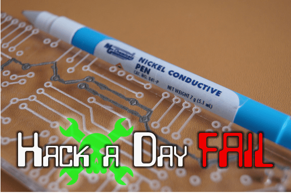
[Frank Zhao] wanted to try his hand at making a transparent circuit board. His plan was to etch the paths with a laser cutter and fill in the troughs with conductive ink. The grooves are ~0.1mm deep x ~0.8mm wide.
He used nickel ink, which is slightly cheaper than silver ink. The ink was among the least of his problems, though. At a measured resistance of several hundred ohms per inch, it was already a deal breaker since his circuit can’t function with a voltage drop above 0.3V. To make matters worse, the valleys are rough due to the motion of the laser cutter and don’t play well with the push-to-dispense nature of the pen’s tip. This caused some overflow that he couldn’t deal with elegantly since the ink also happens to melt acrylic.
[Frank] is going to have another go at it with copper foil and wider tracks. Do you think he would have fared better with silver ink and a different delivery method, like a transfer pipette? How about deeper grooves?
 Fail of the Week is a Hackaday column which runs every Thursday. Help keep the fun rolling by writing about your past failures and sending us a link to the story — or sending in links to fail write ups you find in your Internet travels.


Can copper foil be bonded to the transparent substrate and then etched in the usual way?
Yes it can. At least with glass http://hackaday.com/2011/09/12/glass-pcbs/
Yes i was about to comment i have done exactly that for a project at work (dont ask) simple copper sheet with some heat glue on a pane of glass than a standard DIY etching … … drilling the holes is another story
After reading that article about glass pcbs I wonder how they bond the copper to a standard epoxy pcb?
And I wonder if there might be some sort of reverse-etching process where you put a negative of the trace on the plexiglas to mask the parts that will remain clear, then somehow deposit the copper via sputtering or some similar technique, and as a final step you remove the mask.
“I wonder how they bond the copper to a standard epoxy pcb?”
Using epoxy? :-)
Sustained (apparently hours) periods of heat and very high pressure, apparently.
If you want to do this at home then you probably want to look at “Self Adhesive Copper Foil Sheet”, produced by Venture tape, which you should be able to find at your local stained-glass supply store. I bought some a few weeks ago so that I’d be able to do multi-layer boards whenever I start etching my own boards, but I haven’t started practicing with the stuff yet, so I don’t know if the adhesive would have inconvenient interactions with etchant.
My first choice for multi-layer actually would have been plain copper foil, but I couldn’t even find tin, much less actual copper, and for this article’s subject you might have to figure out an adhesive too.
Another possibility is some metallic hobby paint that’s disolved in xylene ( link: http://www.plaidonline.com/liquid-leaf-copper/89/6160/product.htm ), but once again I haven’t tried it, so I’m not convinced that the stuff is actually conductive (I suspect that you could fix that with an oxidize-then-reduce two-stage process, but I suspect that would likely kill your carrier acrylic too). Does anyone have experience with this paint?
Sputtering might require a plating step afterwards to bring the traces “up to spec”. Also, I think that sputtering usually involves a high vacuum? Maybe painting on some thin graphite ink (or anything else conductive) and then running a “technical pen”( links: http://en.wikipedia.org/wiki/Technical_pen http://www.richardspens.com/?page=ref/design/stylos.htm )-style electrodeposition contact (probably with a non-conductive barrel) over the dried graphite would work better (especially since both steps could be performed with a CNC machine, by just swapping out the tool). Plating is certainly “environmentally impolite”, but it strikes me as much more practical for the hobby market than anything involving vacuum chambers, and apparently you should be ABLE to plate with used etchant (though you should be absolutely paranoid about fumes, even with non-fuming stuff… and then there’s all of the OTHER chemistry concerns: paranoia is good for your health).
If you’re going to sputter anything under vacuum, you may as well deposit indium tin oxide and have the traces be transparent as well :-)
Best solution would be to use a sputtering machine to deposit a few nm thick uniform copper film onto the glass plate and then use electrochemistry to deposit further copper onto it. Then use standard PCB processing equipment.
Yep, copper sputtered on and then etched away.
Of course you will need a very expensive vacuum system to do it.
Dissolve, not melt.
Try a conductive ink that’s more viscous and dispensed via a foot pedal based, air driven dispenser. Akin to how enamel pins are produced. Maybe bake the board once done too?
http://www.youtube.com/watch?v=SN6irpZCpuQ&t=1m19s
Baking the plexiglas is the problem. It can’t stand much heat.
Maybe use wide copper foil tape over the entire glass, then use the laser cutter to “Cut away” the stuff you don’t need, then an exacto knife to pick up the unnecessary copper foil.
Copper has a high thermal conductivity and is moderately effective… Those add up to making cutting clean lines very difficult.
then run it through a vinyl cutting cnc machine instead:
http://fab.cba.mit.edu/content/processes/PCB/vinylcut.html
I have done that. It does work. Expect trace widths less than 1mm to be iffy if you don’t have a new blade. Smallest pitch I could get to work is about .75mm
That would have been my suggestion, too.
You would need a UV yag laser to cut the copper, something very few people have access to.
What about just squeegee-ing solder paste over the whole thing. Kinda like screen printing but not really.
That was my thought,you just beat me to it.
I don’t know the melting temp of acrylic it might melt first. Or, it might just bond together well. Also try etching glass with acid, then squeegee in paste.
I doubt that would work. The solder paste is very cohesive, so I’m guessing you’d get lots of balls of solder instead of it adhering to the acrylic and making traces.
I like the idea of using a transparent medium, it’s pretty “groovy”. Why not just fill in the groove with bare wire…28 guage?
My thought is that this wouldn’t work well for pads, since you want those larger. Of course, if you were willing to mix in a little watch-maker work by using a jeweler’s anvil and hammer to form flattened parts then that would be solved. You could also melt the wire into some forms of plastic, reducing or even eliminating the need for a separate insulating layer.
why not just leave the acrylic’s paper backing on, etch, then go over it with conductive paint?
Use a conductive link that’s *less* viscous (i.e. so it will fill the grooves via capillary action), then flood each channel using a syringe. I’ve watched machinists do the same for machined text using india ink to make it stand out (it was cut into acrylic almost exactly like this). Chances are he’ll get better conductivity, and it’ll look ‘pretty’ too..
To solve the melting issue I suggest using some masking. You can etch the masking and the material with the laser and then apply the paint and or ink. When dr,y remove the mask.
What about trying solder paste in the grooves? I’m not sure the temperature difference between melting plexi and melting solder paste, but I’m sure some innovative hacker could figure out a method :)
At the risk of being rude, it’s not a *bad* idea per se, but the real failure was to not try it with a very simple setup first (eg. a battery, resistor and LED) to see what kind of problems you’d have in making a bigger project. Then the only loss would be a little fabrication time and a few materials.
My thought too. When trying anything for the first time, always do the respective “Hello World.” You don’t build race car before tinkering on a junker.
Don’t want to be a jerk, but this is from like half a year ago, and I remember seeing it here on HaD already, even though I can’t find it now.
Tin Oxide is the transparent conductor used in the manufacture of LCD screens.
Indium tin oxide… But that is a messy fabrication process and the conductivity isn’t that high.
I believe that it’s also fairly expensive stuff.
Print palladium solution onto it with an inkjet, then copper plate using cnc probes to touch each trace.
The problem with conductive ink is while the metal particles are good conductors, they are not continuous. The filler/glue part isn’t too conductive and hence the high resistance. Sometime baking the traces helps a bit, but still not that well. Doesn’t work too well for anything that requires low impedance. Depending on the binding agent and size of particle, traces can crack when flexed.
If your paint can conduct electricity, you can electroplate the nickel paint with a metal. It is a bit of a pain as you have to do individual traces, so you want to have all of the traces connected together, plate and then cut the links.
Could you wipe solder paste across it with a squeegee to fill the troughs, that might be a cheap & easy way to fill the track with something conductive. Wonder if there’s some cunning way of then melting the solder paste without damaging the acrylic?
Maybe with a laser?
One idea, instead of lasering acrylic, sandblast glass. It’ll withstand a higher temperature.
But drilling the thru holes is a bitch.
“Wonder if there’s some cunning way of then melting the solder paste without damaging the acrylic?” Sure there is. Just pick a solder alloy that melts before the acrylic. http://en.wikipedia.org/wiki/Solder
Solder paste would wick right out of the grooves. It won’t wet to the glass, and as soon as you put a component in that it will wet to, it would wick up and the ‘trace’ would be broken.
Oh right…. even if you populate you still have wicking. I was surprised how much solder was used when I switched to paste. Not too practical but maybe find a way to pre-tin the components, place, then melt the solder traces?
Indium based solders will wet glass.
Gallium based solders also wet glass.
True, although as a practical application I don’t think you can buy indium solder paste (indium-the-metal, not Indium-the-company). You’d need one of the alloys (…or maybe just indium itself) that has a moderate temperature melt point, too.
You could try curing it with hot air from a blower (no, not that hot, you don’t want to find another way of melting plastic). Curing conductive ink can help the resultant conductivity – and drying it faster should help avoid so much chemical attack of the plastic.
What about using a light graphite paste then electroplating copper. That has its own problems.. All traces need to be connected to one bus but hey.
Same problem as the ink, high resistivity.
Not after you plate it with copper.
I played with MG Nickel Print around 15 years ago. Assuming the product is the same and my memory’s still good on the topic, it took more than a day for the resistance of a decent thickness to decrease to the final value. Don’t expect miracles from such a cheap conductive ink, but make sure you don’t test too soon.
Perhaps it’s possible to apply a coating/sheet of something to the acrylic that can be etched by the laser, and resists the ink solvent. Then remove it after applying the ink, taking the overfills along with it.
Or perhaps after laser etching, apply a thin coat of something mildly conductive to the entire surface of the etched side. Electroplate the entire surface with copper. Then sand and polish the surface, leaving only the copper in the lower etched areas. Could work if the laser can make the etched areas deep enough.
Alternately, after copper plating, apply a resist to the entire surface. Sand away just the resist on the raised areas (not the copper), or have the laser remove it by burning a negative image. Then etch chemically. Assuming the acrylic is undamaged by the process and chemicals, it would save you from having to polish the acrylic back to clarity.
What about ultrafine copper powder? (Ascorbic Acid + a copper salt). Put the powder in the paths and anneal.
Acrylic starts to get all melty at about 140C.
Maybe multiple parallel traces to reduce resistance in critical parts of the circuit?
Curious would laying a sheet gold leaf work by gluing up the traces and working it in?
Id imagine it wouldn’t rate too good on the flexibility factor but it would still be transparent…
I tried something similar not too long ago lasering deeper groves into thin acylic that i tried to, inlay, so to say some very thin wire, then i laser cut holes and used through hole PCB components, the main problem came with inlaying the wire, the laser channels were not quite deep enough, and also the act of soldering the through hole components, while functional, tended to melt the acrylic around the hole. It ended up working, but not quite as sexy and i wanted, lol.
It seems to me that, due to the depth of the etching, he could have applied a conductive paste (of a very carefully selected variety) by squeegee, the way a scoop coater works in silk screening. The etchings would be filled and he could work on removing excess from the surface during a later step. If the material properties were chosen *just right*, the traces might be made to reflow and solidify without destroying the substrate.
The bigger question is this; for what purpose would a pcb need to be transparent??? It seems like allot of effort just to end up with the PCB equivalent to the 1980’s phone sets in the clear housings. Kind of gimmicky.
I think it could look pretty cool, personally, since things are cleaner and more condensed than those days. Especially if the traces are laid out nicely. You could make a slick one-piece touch interface/LCD cover with capacitive pads on the back, with protected indicator lights and such.
It’s been done with copper tape on glass, acid etched and reflowed. The guy who did it made a Minecraft server on a microscope slide (with microSD slot, ICSP header, ATMega328, and a Microchip NIC, magnetics, and RJ45 jack for a LAN connection).
A squeegee sounds like a quick way to get it done right, perhaps with some sort of UV-curing conductive paste. But you’d need a really low melting point solder to stay below the melting point of acrylic (320F/160C) as well, so even if you could make the board in acrylic you might destroy it trying to populate it.
album and discussion: http://imgur.com/a/6ePKc http://redd.it/136356
demo video and more discussion: http://redd.it/138cvg
The gold leaf suggestion is great, but that stuff is oh-so thin… not sure that would meet the conductor’s physical requirements. Otherwise, combining the two processes, adhesive could be scoop-coated on, the board surface could be cleaned and then a sufficiently heavy gold or copper leaf could be applied. The trace edges would probably end up super crappy looking but it might still make something blink-n-buzz.
I noticed in my kids model paint kit they had a bottle labeled “Clear”. So couldn’t this guy just do a regular circuit board and then paint it “Clear”?
dissolve graphite in alcohol and a low resistance binder agent and a use the screenprinting method stated above on a hello world circuit
I’ve done this a few times, I just mixed a load of graphite powder with PVA glue and squeegee’d it in.
How about using plating methods to provide a base simular to what they at caswellplating.com according to them you can plate tin on to platic using a copper paint based
What they say about it is Coat with Copper Conductive Paint, dip in Tinning Solution, plate with Acid Copper, then Tin Plate.
Prehaps the copper conductive paint and then plating it would help, or the copper conductive paint itself
There’s a flaw in your cunning plan – isolated tracks.
You’d have to do a custom bed of nails type thing to get all the traces energized for plating. A pain for sure, but possible.
And you’ve just plated your bed of nails to the part.
This conversation has occurred many many times… “but what if….” is always followed by “No”.
Well, there are conductive silver inks that are intended to be applied on polymer surfaces (PC, Silicone, Vinyl ‘n stuff), you could probably try these since they probably won’t dissolve the substrate.
Why not use Graphite Paint then copper plate them? Actually I would be interested to see what would happen if you etched it, dusted with graphite, etched again then dusted with another layer, etched again… etc… would this build up a enough of a layer in to the plastic to become conductive to then be copper plaited rather than just painting.
I recall reading about PCBs made from adhesive copper foil going back as far as the 1970s. Does this not exist any more?
Not the thin stuff.
Smallest size is 5mm wide (a bit under 1/4″) and that’s usually for for making stained glass lamps & stuff. For cutting it thinner yourself, read up on pinstriping (as in painting).
They’ve only stopped making it (or run out of old stock) in the past few years. Just as I wanted some, of course.
Could possibly use gold leaf to do this as well, you would have to just be careful as gold leaf is generally not actual gold. Another option would be to lay wire into each track then put a layer of clear epoxy over it to fill it in, leaving a small loop on each end to solder too. This would create a “wire inside the board” effect and possibly allow you to do several “layers”.
Wouldn’t thin transformer wire be less visible and have less resistance?
…and is coated in varnish that may present a few difficulties.
What about build the circut flat deadbug and then epoxy cast it?
what about this way? Graphene doesn’t react much with a plexi afaik.
https://www.youtube.com/watch?v=WZgwTrJS8BU