[Charlie] was killing some time hacking on some cheap FPGA dev boards he bought from eBay. Initially, he intended to use them to create HDMI ports for a different project before new inspiration hit him. Instead, he added an HDMI port to Neo Geo MVS games. The Neo Geo MVS was a 90’s arcade machine that played gems like the Metal Slug and Samurai Showdown series. [Charlie] has a special knack for mods, being featured on Hackaday before for implementing Zork on hardware and making a mini supergun PCB. What’s especially nice about his newest mod is that the HDMI outputs both audio and video.
[Charlie] obtained the best possible video and audio signal by tapping the digital inputs to the Neo Geo’s DACs (digital-to-analog converter). The FPGA was then used to convert the signals to HDMI, maintaining a digital signal path from video generation to display. While this sounds simple enough, there was a lot that had to be done. The JAMMA video standard’s lower resolution was incompatible with the various resolutions offered by the HDMI protocol. [Charlie] solved this problem by implementing scan doubling using the RAM on the Cyclone II dev board. He then had to downsample the audio to 32kHz (from 55.6kHz) in order to meet the HDMI specs. Getting the sound over HDMI required adding data islands to the signal, a feat [Charlie] admits was a frustrating one.
When he tested the HDMI with his monitor, it was out of spec but still worked. His TV, on the other hand, refused to play it at all. This was due to the Neo Geo outputting 59.1 fps – not the standard 60 fps. Using the FPGA, [Charlie] overclocked the NeoGeo by approximately 1% and used the 27Mhz pixel clock to change the FPGA output to a 720 x 480p signal.
For those that love the scan lines of yore, they can be enabled with the push of a button. [Charlie] notes that there are some slight differences in the shadow effects of some graphics, but he has done his best to minimize them. He also admits that the FPGA code contributes only 100 microseconds of delay compared to analog output, which is fast enough for even the most hardcore gamers.
Check out the video after the break to see how the Neo Geo looks in HDMI along with a side-by-side comparison to a CRT TV.


this is brilliant, and I love it. thank you!
Thanks for featuring my project. A small correction though, it’s 100 microsecond delay not 100 milliseconds (which would be bad!). That’s the delay going from the pixel being generated to it being transmitted over HDMI. The TV/monitor might introduce an additional delay though. My monitor seem to be around a frame (16ms).
Thanks for the update, I was shocked that an FPGA would introduce that large of latency. And surprised that no one seemed bothered by it.
The only way an FPGA could introduce a 100 ms delay is if it was intentional.
Oh no, now I can’t just claim that audio-over-HDMI is too complicated to avoid adding it in my project! ;)
Thanks for releasing the code. Do you mind if it is re-used/re-implemented by others? Your project doesn’t seem to specify any license, so that would technically be prohibited right now.
I don’t mind at all. I normally release stuff under BSD but in this case as I started out with someone else’s code (the DVI/HDMI sample on fpga4fun.com) I don’t know what the legal situation was so didn’t add anything explicitly. I asked Jean’s permission to publish and he was happy for me to but I didn’t ask about applying a new license to it. There’s not too much of the original code left but I’d like to give him credit for making a nice sample to start with. I could ask him about realising under a proper (free, do what you like) license if that’d be useful.
Fixed! Sorry about the error – I edited Theodora’s post and missed it myself.
Hi, Charlie. I watched your video a few times and you clearly say microseconds. I even asked my editor if I was missing something because the latency seemed very long. Apparently my brain twisted my synapses into a balloon animal last night (likely a giraffe with its head stuck in a tree). I really enjoyed covering your project; sorry for not doing it justice!
No worries! Just thought I’d get in before all the comments were about the lag being awful :)
Kudos and good job, Charlie. You solved some funny problems and updated a classic. Keep up the good work and I will have to look further into the fpga world of fun.
Might sound odd, but you should tweet (or something) the Giantbomb guys about this, I could imagine them being interested.
Since displayport is always at least 6 months ahead of the HDMI standard isn’t that the ‘standard of the future’? And HDMI is the standard of the now, since unfortunately it won out in acceptance (so far).
In that case, did it replace BetaMAX? Since when does technical merit matter?
Eh, display port is getting more common, and I suspect as 4k starts to become popular displayport will be necessary for devices to do things like 3D properly
From the wiki:
>The DisplayPort connector can have one, two, or four differential data pairs (lanes) in a Main Link, each with a raw bit rate of 1.62, 2.7, 5.4, or 8.1 Gbit/s per lane
You can’t generate that on FPGA without a SERDES. I have yet to see a FPGA with SERDES outside of BGA and the old ball QFN packages. DVI/HDMI on the other hand have lower speed modes that can be generated on a FPGA and you can even buy chips to go from LVTTL to DVI/HDMI at QTY 1.
wow! extremely cool!
Awesome work, thanks for sharing your code.
Thanks for sharing!
Very nice work indeed!
Any Links to the FPGA he used?
They are EP2C5 mini dev boards. Just search for EP2C5 on eBay, there are loads of them. They are great boards, I’d highly recommend them. Very cheap if you can wait for them to come from China. You’ll also need an Altera USB Blaster which you can get for eBay too for around $6.
Thanks for sharing the details !
I see that you are using a small board with an HDMI connector. Is that a plain breakout board or does contain an HDMI transmitter too ?
It’s basically just a connector. There’s two pull up resistors hidden under there but that’s all. It’s the part of the project I’d definitely change if I was to do it again. I had some adapter boards (TQFP to DIP) which had the same 0.5mm spacing as the connector so I just soldered it to that. In retrospect it would have been much more robust to buy a HDMI extender cable, cut it in half and use that as a socket. After repeatedly plugging and unplugging the HDMI cable the solder joints have started to fail and now only works reliably due to the pressure applied to it by being screwed to the backing board.
Oooh… I have a *pile* of MVS single slot boards… (In addition my 4-slot cabinet) I’m going to have to look into this for consolizing a couple of them. :D
Reblogged this on Alexander Riccio and commented:
A brilliant hack. And available on GitHub!
You can always convert the audio to analog then back to digital at the right sampling rate.
not bad
Son, I am apoint, I am very apoint.
‘Apoint’? Is that meant to be the opposite of ‘disappointed’?
Had to downsample the audio for HDMI? Somewhere an audiophile is gnashing, or writhing, or cringing something.
My HDMI cable doesn’t even have gold plated connectors! Shock horror!
Dear god…and… Less (thinner) than oxygen-free 8 gauge solid copper per strand?!!
There’s a special hell reserved for heretics like you
Great project, very exciting! I am interested on doing this for my MVS for when I consolize it. On the git repo, I see wiring details for the SvC board – do you know if those match up to a standard MVS board? I’d be doing this on a MV-1B.
The SvC board didn’t match the MV-1FS schematic (https://wiki.neogeodev.org/images/7/72/Mv1fs-page3.jpg) but was fairly easy to remap. I first looked for some 74LS273s near the JAMMA connector and then measured the resistance between the outputs and the R/G/B JAMMA outputs to work out what output each was driving (I made notes on the wiring doc of what I measured). If yours doesn’t match the schematic either then you can repeat this process. Only thing to look out for is that the SHA/DAK connections need to be on the respective input port of the 74LS05 because the outputs of that chip are open collector. Hope that helps.
Little late but I’m trying to set this up for myself and wanted to clear a few things up.
Can you clarify the following from the github project re: wiring?
“All lines go through 500Ohm/1KOhm resistor voltage dividers to get from 5V input to 3.3V output. Except NEOGEOCLK which is the only output from the FPGA and drives OSC input directly.”
I read this to mean that each output from the NEO GEO goes through a resistor to the FPGA. Is that correct?
“INCLK goes through the PLL to generate 27MHz (pixclk) and 135MHz (pixclk72). SWITCH needs the weak internal pull up set to work.”
I’m not sure yet what this means.
Thanks!
I’ve figured out most of it. The voltage dividers take all the lines from the NEO GEO board and push them down to 3.3V.
The thing is though I don’t measure anything near 5V on any of the lines. Is this expected?
Also figured out that INCLK is the FPGA clock pin, and the SWITCH is the internal FPGA button.
I could not get any HDMI output however, and can’t tell yet if this is a wiring issue or a FPGA issue. The FPGA is outputting the NEO GEO clock signal, which I was able to test.
Would it be possible for you to put up detailed pictures of the PCB and wiring?
OK, sounds like you’ve worked most of it out already. The resistors are voltages dividers so each input from the Neo Geo goes to a 500Ohm resister (which I made from two 1Ks in parallel as I had lots), then to a 1K resistor then to ground. The FPGA input is taken from between the two resistors. Strange that you aren’t measuring 5V on the lines, the ICs are simple logic gates so as long as the power rail is 5V they should output something close to it. How are you measuring it?
If you aren’t getting any input then the first thing to try is ignoring the video sync from the Neo Geo “sync” (ie. change “if (sync) begin” to be just “begin” and reprogram the FPGA). This will mean that you should get a valid HDMI signal out at least (although might be a black screen). If that still doesn’t work then it’s likely nothing to do the the Neo Geo side of things and something wrong with your HDMI wiring (you could unplug the Neo Geo side of the connector to rule it out completely) at that stage.
I’ll try and get you some photos tonight. I would rather not have to dismantle it though so not sure how much additional information they’ll be over what you can see in the video.
Your description of the voltage divider is the same conclusion I came to as well – that’s how I wired it up on my breadboard, using the input and a shared ground – however I had to use slightly smaller resistors as I did not have many 1K or .5Ks sitting around.
I was measuring the voltage using a multimeter, going from ground to the respective pins on the 74ls273s and 74ls05 outputs. Normal RGB output is still working so nothing is damaged on the board.
I will be attempting another go at it, as I have some concerns looking at the solder on my pins that I may have hooked sync up to pin 20 instead of pin 1 on IC7, and will re-confirm the resistance at the outputs to ensure I grabbed the right ones. I will also give the sync-check disable code change a go as well to see if I get an HDMI signal.
If taking detailed images is going to cause damage to your setup please don’t worry about it – I should be able to make do without them.
Thank you – you’ve been a great help.
So I did some more work on it and confirmed the HDMI port wiring. I’m using a project-board type HDMI port that plugs into my breadboard.
All of the HDMI output pins measure ~1.5V. Everything is wired up as indicated and I don’t see any shorts on the board itself.
After replacing if (sync) begin with “begin”, I still get no HDMI output. I’ve tried multiple displays and HDMI converters that otherwise would work.
When programming the FPGA, for a moment after I do manage to get a screen blank at random so perhaps the signal is good.
I am however starting to question my FPGA and Quartus configuration (mostly because of my inexperience in the platform).
The project compiles and the pins in Quartus all match up. I’m using a EP2C5T155C8N. When the FPGA is programmed the 3 LEDs go from flashing to lit, although the 2nd one is dimmer.
There are a few compile warnings (no errors) that bother me, such as (truncated for brevity):
Warning (272007): ALTDPRAM doesn’t support Cyclone II.
Warning (306006): Found 9 output pins without output pin load capacitance assignment
Warning (169174): The Reserve All Unused Pins setting has not been specified
Warning (10230): Verilog HDL assignment warning at HDMIDirect.v(88): truncated value with size 32 to match size of target (24)
So, assuming those warnings are truly benign, I’ll keep at it some more and try wiring the NEO GEO board back up for another go.
The compile warnings should be fine, I get a bunch of them too. Can’t remember the ALTDPRAM one but I can check it later. The LEDs sound like they are lighting up like I’d expect them too. And you’re reading 1.5V at the output pins which sounds good as half the time they will be near 3.3V and half the time near 0V so averaging around 1.5V sounds about right. (This is also the reason you don’t see 5V on the logic ICs on a multimeter by the way). So, the FPGA programming side of things sounds good. You also said you measured the Neo Geo clock output before and it was good? Are you programming via JTAG? (I found if I did active serial programming I had to pull the programmer out before it’d run but JTAG was fine).
With the sync line taken out the Neo Geo side of things shouldn’t have any effect, so must be something up with the HDMI side of things. Are you absolutely sure all the grounds are connected correctly? And you’re getting 5V on pin 18? I’ll double check the wiring table tonight to make sure it’s correct. I know I connected pins 15 + 16 to the 5V pin via 1K resistors (to act as pull ups) but I would have suspected leaving them unconnected would have been fine too.
PS. You could also change the “red <= 0;" lines to be "red <= 255" to make sure you should get something on screen (other than black) even if the neo geo side of things wasn't working.
Charlie,
I did confirm the NG clock output works by running the FPGA pin 64 (I think that’s the clock pin) to the xtal pin on the NG board – it would boot up with a good picture over normal RGB using that (and wouldn’t without the xtal installed of course) so I assumed the clock functionality of the FPGA code is working properly.
I am programming via JTAG but once I get things worked out I have an advanced configuration memory chip I’m going to install to keep the code in memory.
I definately got 5V from pin 18 and any other pins that were expecting 5V. 15/16/ are connected to 5V via pull-up resistors as well. All of the grounds are running to the main ground on the FPGA (I’m using the power header from the FPGA to connect the breadboard to +5/GND from the FPGA). I’ve run through the HDMI cabling about 3 times already so I believe that is good.
This coming weekend I’ll be able to wire it up to the NG board again and give it another go.
I will try the “red <= 255" change to try and get some HDMI output tonight though.
Thank you!
Karl
I was able to try setting the red value to <= 255 on both lines but still no output. Based on your input that should present me with some sort of HDMI output.
Regarding the HDMI port itself, I was able verify that all pins have connectivity by doing continuity tests on the breadboard through an extension cable – all pins matched up as expected.
Would it be possible for you to add the sof/pof files to the github page, so I can rule out any programming issues?
Regards,
Karl
Yes sure, they are on github now.
I just tried recompiling and I definitely don’t get the warning about ALTDPRAM so maybe you are on to something. Although even if the RAM wasn’t there it shouldn’t stop the HDMI signal being produced. Who knows what else could be going wrong though.
Another thing you could try would be commenting the entire contents of the “always @(posedge pixclk)” section that starts with “AudioPacketGeneration();”. Without that section it’ll be just a standard DVI signal (no HDMI data packets like the audio).
I also started putting together a new HDMI cable for a new project so I’m doing it from my own wiring table as a way of verifying it. Was hoping to get it done last night but it took longer than I expected. I’ll finish it off soon though and let you know. The new one will be easier to take photos of too.
The only thing after that would be some sort of analog issue. The HDMI signals are probably pretty fast to be trying to run through a breadboard (I don’t think they are recommended to be used above 10MHz). The analog domain isn’t really my forte, I just tried with a floppy drive cable and got away with it but I might have got quite lucky.
Thank you, that is great! I’ll try the files when I get back to my workbench on Friday.
You make a good point about the analog issue… I have some direct-solder HDMI ports that I’ll put together to attach to the FPGA and bypass the breadboard.
Karl
I finished my new HDMI cable off tonight and so verified that the wiring information I gave is correct. However, and I feel really bad for not checking this properly in the first place, I told you the wrong bit of code to change to remove the sync with the Neo Geo video output. I made my new cable, made the change to that line, programmed a new FPGA and it didn’t work for me either. You need to remove or comment out the whole “if (sync) begin ….. end” section. Commenting out just the “if (sync)” had the opposite effect than I intended and meant it’d always think it was out of sync and so didn’t produce the video signal. Sorry for leading you down the garden path on that one.
Glad to hear the cable worked out, and no worries on the syntax mix up. I think that tonight maybe I’ll actually get some HDMI output!
Removing the whole if (sync) begin … end section did it – I’m getting HDMI output! So now that’s ruled out I’ll be wiring the MV1B board back up.
Thanks and I’ll keep you posted.
Charlie,
I’ve made lots of progress. I have everything wired up and have OK video output. I say “OK” because largely it looks quite bad because there is color bleeding related to some sort of sync issue. (I’m really happy to have any video but I want this to be playable at some point)
Oddly, when I touch the SYNC output that goes to the FPGA with my multimeter, it clears up. Did you have any particular issues with SYNC?
Additionally, I cannot get any sound output. My board has a YM3016 DAC. I’ve found the clock and data inputs on the DAC, but now the LRCK. I’ve tried every pin on it and I can’t get any audio.
Looking at the video the DAC on the SVC board is similar to the MV1C, which is a 9480F.
Can you confirm this?
Excellent news! Congrats!
The SYNC line effecting things sounds odd. The only thing it’s used for on the FPGA is mainly just for centring the picture, not anything to do with the picture data itself. It does effect the HDMI timings if it doesn’t get the SYNC at the right points (the bit of code you commented out) but I would expect you to just get no signal in that case. However, the SYNC line is connected to the clear lines on the 74LS273s so I’d assume it’s something in your set up that’s affecting the operation of those chips. Have you tried disconnecting that line (you should still see a picture if you have that bit of code commented out)? Also are all your grounds connected correctly (ie. Neo Geo ground and FPGA ground are the same)? If that doesn’t work then can you post a picture of what you’re getting?
You are correct about the audio DAC, it was a BU9480F (http://pdf.datasheetcatalog.com/datasheet/rohm/bu9480f.pdf) on the SvC board. Having a hard time coming up with decent info on the YM3016. Looks like SMP1 and SMP2 do a similar job to LRCK but might not be exactly the same. If there’s no datasheet with info then it’d probably be easy to check what it’s doing using a logic analyser or an oscilloscope and try and work it out from there. I could do that for you if you don’t have one.
Yeah you are right about the sync – disconnecting it gets me a off-kilter image, but the same issue still stands. That said touching it with my multimeter doesn’t clear it.
My grounds are all on the MVS board, going to a central point. The FPGA and the sub-board with the resistor voltage dividers connect to ground at the same location.
Here’s a good pic of the bleeding color. Earlier, this would line up and look *perfect* when I touched the SYNC output pin with my multimeter … really weird. I’m thinking of adding a cap between the
http://tapatalk.imageshack.com/v2/15/03/13/a32b42addfee8a98fee74a18b2c54644.jpg
I got to thinking about the clock signal wire causing issues, so I used a solid core wire and made it as short as possible – I also wrapped it in a ground wire going from the FPGA to the ground at the original xtal location.
Here’s some information on the YM3016. Any help with the sound would be appreciated as I’m at a loss there for the time being.
https://wiki.neogeodev.org/index.php?title=YM3016
So, some really good news.
I was able to get a perfect picture by running a wire from the FPGA sync input, to a heatsink on the mainboard. This seems silly to me but it works perfectly.
There were some red artifacts on my newer display, however those disappeared completely once I assembled the FPGA board into the case.
My take is this setup is sensitive to interference, but once its stable it’s perfect.
Here’s a pic, and I’m posting a youtube video up soon.
http://tapatalk.imageshack.com/v2/15/03/14/cdcd07e7917ebdc00a1e06ba050e7d84.jpg
Excellent! Congrats Karl! Looking forward to the video.
Bit weird about the heat sink thing but if it works…
Bit of a problem with probing the sound on my Neo Geo as I’ve just found my power supply has failed. Will probably have to wait for a new one until I can do it now. Hopefully this week though. I found a datasheet for the YM3012 which had the info I need and probably is the same as the YM3016. I could try changing it blind but it’s probably easier to wait.
BTW, I just pushed a new branch to github (ui), it adds a splash screen, an error when not syncing and a message showing what scanline method is currently being used. It’s not on the master branch yet as I haven’t been able to test it due to the power supply issue. But if you’d like to give it a go I’d appreciate your feedback.
Thanks! Here’s the video. It’s just a short video of the Metal Slug X attract mode.
http://youtu.be/uwHHyxcF7LU
Regarding the Ym3016, do you think it’ll require analysis and additional coding? Or is it a matter of matching up inputs?
Sucks to hear about the power supply. You can use any 5V+ power supply, the one I’m using is an AES power supply. It does 5V @ 3A, though less than 3A will probably work.
I’d be happy to try out the new code, I’ll let you know how it goes.
Karl
Looking at page 4 of the schematics, I can see the YM3016 and it has 4 inputs – SD, CLK, SMP1 and SMP2. I’m assuming this chip gets its audio data differently from the 9480, and that the channel data that would be in LRCK held in the SMP1/2 signals.
https://wiki.neogeodev.org/images/9/9c/Mv1fs-page4.jpg
Thanks for the video, it’s good to know someone got something good out of me sharing the code. Looks like a really nice picture. Just need to get the sound working now!
I remembered I had an old super gun, so I did get to probe the YM3016 on my cartridge based MVS. Looks to match what I saw in the other YM301X datasheets (ie. http://www.datasheetlib.com/datasheet/735270/ym3015_yamaha-corporation.html?page=7#datasheet). It will need some small amount of extra code to get it right. It’s not many lines, I’ll hook up some connections and test it out.
Not perfect but try changing two lines in the audio input section to…
always @(posedge audioClk) audioInput[0]>1)|(audioData<<14);
always @(negedge audioLR) begin curSampleL<=audioInput[0]; curSampleR Pin 4
– audioClk (pin 120) -> Pin 5
– audioLR (pin 114) -> Pin 8 (or Pin 7 for audio from the right channel)
All through voltage dividers like everything else. The YM3016 pinout didn’t seem to match what the internet thinks it is, at least it doesn’t match the YM3016-D on my MV1-FS.
I’ve got to play with it a bit more to get it working nicer and add stereo but will leave that until tomorrow.
That got managed by the comment system.
audioData (pin 118) to Pin 4 on the YM3016.
And the second line of code is
always @(negedge audioLR) begin curSampleL<=audioInput[0]; curSampleR<=audioInput[0]; end
Cool! I tried the audio changes and I get audio output, although it is distorted – sound like it’s too loud. But it does sound right besides that, so that’s great! How would it be toned down?
I also tried the UI code, I like the boot splash and the scrolling error messages. Although now with that code I get “bad sync signal” messages and the screen position is messed up. That is using the newest SOF file from your github. Similar results when I compiled myself.
Went back to the original SOF file and it’s fine again. Not sure yet what changes would impact the sync signal yet.
The distortion might have been caused by latching on the wrong edge or not being centred around 0. I’ve made the necessary changes and uploaded to github if you want to try it out. I’ve also added stereo decoding, you’ll just need to connect up one extra line (details in Wiring.md). I also added some defines so you can enable/disable stuff like the sync error (BAD_SYNC_DETECT), the splash screen and the delay before the splash screen starts. The bad sync error comes on and stays on so maybe you’re getting some bad syncs at the start but then it clears up, so you might want to just comment out the “`define BAD_SYNC_DETECT” line towards the top of the file.
Charlie,
I was able to test the updates and the sound works perfectly! I need to verify that the volume normal, but otherwise it sounds great. You are the best!
The only oddity I notice is that if I turn the system off, then back on without disconnecting the HDMI cable I am presented with a sync error. I’m expecting this has something to do with the FPGA not powering off completely due to power from the HDMI connector but I’m not sure yet.
I’m going to play with the splash screen, sync errors, and NEO GEO screen dimensions (to see if I can get full screen) later tonight probably.
Also, in my previous testing the button on the FPGA board would not change scanline settings. I should try that again too.
BTW Thank you for all your help. I know this started as a “hack” but you’ve gone above and beyond to help make this more available for the NEO GEO enthusiasts.
Karl
Also,
The extra pin for the YM3016, you have as going to pin 116 on the wiring document – there is no pin 116 on the FPGA.
I assumed you meant 112 and wired it there, and confirmed this in the pin planner for the project in Quartus, so the wiring.md needs to be updated.
Hey Karl,
Glad the sound worked!
I shared the code in the hope that other people would use it so I’m happy that someone did. You’ll have to keep me updated if you’re doing a full console conversion.
I noticed the “oddity” too. It does seem like the FPGA is getting powered via the HDMI cable somehow, keeping it partially powered up. Looking at the FPGA dev board schematic (http://www.leonheller.com/FPGA/EP2C5T144mini.pdf) it seems my use of pin 73 is dodgy but as it’s related to the HDMI cable being connected it doesn’t seem to be that. I can only think it’s Pin 7 which is the problem in that case. If there’s a pull up on the HDMI data line then it could be powering via the reverse biased LED. It’s not good that an LED is on a data line so would be good to move anyway.
The button debounce code used to use the audio clock as it’s clock source which would explain why it wasn’t working in previous version. When experimenting with the UI I changed it to use the pixel clock as I didn’t have a Neo Geo connected up. So, in short it should be working now :)
Tweaking the screen dimensions would be tricky code change. Scaling along the X axis wouldn’t be too bad but scaling on the vertical would be hard as I’m not sure the FPGA has enough memory to make it possible to scale up more than a couple lines. Also I’m not sure how good it’d look as they’d be a non-integer scaling.
Audio should be easier, something like…
always @(negedge audioLR) begin curSampleL>N; end
And the same for audioLR2. Where N is some integer (1 will half, 2 with quarter etc). You will be dropping the least significant bits off the audio data though.
Charlie
PS. You were right about the pin numbering mistake. I knew it was on one side of 114 :)
Thank you, the scanline button is working now, it’s great! Although I prefer the default option anyway, but it’s still cool to be able to change it. I wired it up to a button on my MVS.
I will try re-routing pin 7 to another pin to resolve the HDMI power issue.
Looking at the FPGA board schematic though got me thinking about my SYNC line oddity, where the image clears up by having SYNC connected to the heatsink.
On the schematic, it says pin 104 is PLL2, vs LVDS like the other inputs. Is this intentional?
FYI I wired up a controller port and actually got to play some games on it. It looks and plays great so far!
Hey Karl,
I think pin 104 should be OK. It seems to be marked as IO, PLL2. I’m just using it as an IO pin but it looks like it can also be used as a dedicated route out for one of the PLLs. Still not really sure what’s up with your sync issue. Hopefully I’ll be able to recreate it when I get around to modifying my MV1-FS.
By the way, did you have any luck with the HDMI power issue?
Charlie
Hey, I was just about to leave a note here.
For the HDMI power issue, I tried removing pin 7, but even with that pin removed the FPGA stays powered on.
In that situation, I measured 2V across the data lines on the HDMI port. (They measured 3V with everything off). Would diodes be required to keep the datalines from feeding back into the FPGA?
For the sync, I moved pin 104 to a non-PLL in and it didn’t change anything. My picture still looks bad, until I connect the sync line to the heatsink or any other non-grounded object (Such as a screwdriver, multimeter lead, etc), which I find quite odd. Even if its disconnected, if I momentarily touch such an object to the sync line, it clears up instantly. It’s really weird. I do hope you can recreate it as the hardware should be similar, but my MV1B is in somewhere between the MV1FS and MV1C in terms of design – it wouldn’t surprise me if the problem didn’t come up.
My best guess is that it has something to do with the clock signal going to the NEO main board. How would I go about disabling it and using the actual NEO clock signal for testing? How are you shielding the clock signal on your MVC board?
I’d like to try an AES system next as they have great shielding around them and I’m wondering how my problem would behave on those.
Karl
I’ve also noticed that in scenes with a lot of on screen action or flashing, I will get a line on the side of the screen. I’ll try and get a pic of it. I know it happens for sure in Fatal Fury 2 during the opening sequence.
Hey Karl,
This weekend I got round to doing the mod on an MV1-FS. Found some issues which might be of interest to you so I thought I’d best let you know.
First thing I noticed was that the clear line on the 74LS273s (the SYNC line) wasn’t behaving the same as on the SvC board. It was only asserting during (a slightly extended) vertical sync whilst the SvC board would clear on both horizontal and vertical syncs. As you did get a centred picture I’m inclined to think maybe your board uses the new style clear but maybe they are all slightly different. I was confused by why the clear line effected your picture at first but thinking about it now it’s using it to synchronise to the pixel clock (once every 4 24MHz cycles). I also had to change the trigger to the positive edge of neogeoclk to get it correct (the phase of the clock seems flipped).
I noticed the wiring info had another mistake in it too. Pin 99 SHA should have been 150 ohms to the red output. Also, as it’s open collector output for the 74LS05 I used the input to the gate. Therefore you need to find that pin but then wire it to the input pin for that gate. If you wired it by finding the resistances then the shadow bit will be having no effect.
On the MV1-FS I’ve been having a bit of a nightmare with the clock line. Tried so many configurations today of different shielded wires that I’ve lost track about where I’m at with it. In summary, it seems I’m able to get to around 75% of normal speed and everything works fine but beyond that things start getting flakey. Was thinking at first it was interference but I now wonder if it just doesn’t like the over clock (as it’s done in jumps which means occasional parts of the duty cycle are 27MHz). Need to probe it properly but it’s a bit of a pain as everything is underneath the shield and probing the output of the clock pin seems to effect the result.
Anyway, I’ve pushed my (small) code changes to a new mv1fs branch on github. You might just want to examine the code changes instead of the whole project though as it’s committed with the slow clock and pin 73 moved to 104.
Charlie
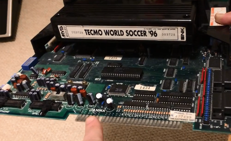
PS. I noticed a line down the very left hand edge of the picture on my test game (Tecmo World Soccer ’96) but this was just down to not prefetching the line doubler RAM far enough in advance. Hopefully is the same one you were seeing. Was a one line fix and on the branch too.
Thanks Charlie,
I’m going to be trying this on a 2 Slot board which should be similar to the MV1FS. I’m guessing I’ll see differences in the SYNC line when I get to do it.
For the SHA connection, I think I noticed that difference and went with what made sense according to the schematic… I’ll double check though.
My clock line gave me lots of trouble too, mine as it sits is a solid copper wire soldered to the FPGA and the main board, wrapped with a +5 wire from the board and GND from the FPGA.
I’ll check out the code changes when I get a chance.
I’m glad to hear you’re trying it on another board and haven’t been put off too much with your troubles on the last one.
Haven’t had much time to do stuff today but I did try a more subtle overclock scheme this morning (50/50 duty cycle 24.54MHz) and that seems completely stable. Just need to do some adjustments to get it to vary the overclock to get exactly 60fps but looks like it’ll work. The newer Neo Geos probably have better tolerances so would accept the cruder method I used before.
For the clock line, I tried coax aerial cable and my own home made coax but neither seemed to be as good as just using some multicore alarm wire with everything but the central line connected to ground at either end. It was a pain to get right but I think the setup I have now is good. I couldn’t find anywhere good to mount the FPGA apart from on top of the cartridge slot so ended up having to have a longer clock line that was ideal.
Hoping to get this finished off soon. Definitely by the end of the week as long as there’s no more surprises. Then I do some brief documentation on it.
Nah, I certainly haven’t been put off at all – this is a fantastic mod and it seems the more we tinker with it the better it gets… and I love tinkering, time allowing for it.
You’ll have to send me some details on the “alarm wire”, does it go by a brand name? I was thinking of trying coax as well.
To mount my FPGA I used nylon stand-offs and just had it sitting on the board, eventually glued it in place. On the MV1FS you should have plenty of room for it under the cart slot… but that’s just based on images though so it’s conjecture at this point.
Can’t wait to try the new code for the adjusted clock, I have a feeling that will solve my weird sync line problems!
Thanks!
Karl
Good stuff! :)
I got my MV1-FS working well yesterday with the correct overclocking and the picture looks good and steady. Haven’t hooked up sound yet, a job for tomorrow (although not expecting to hear much as part way through repairing the sound system on that board). Need to test the code with my original build to make sure everything works still with that then I’ll merge that branch back into master and update the surrounding documentation. It’d be good to have the pinouts of the MV1-FZ too if you kept a record so we can list them all in one place.
The alarm wire I was talking about is just the stuff you get for burglar alarms. I use it mainly because it’s a cheap way of getting 8 or 12 different colours of wire. Nothing special. For the clock line, I used the central wire and then connected all the others to ground. It seemed to be the correct balance of shielding and capacitance to allow the signal to get through. I’d be tempted to try a differential pair if I were to do it again though.
I planned on mounting the FPGA under the cartridge slot at first but decided on using dupont connectors for everything which ended up being higher than the floppy drive cables I’d used before. Only place left that didn’t block the cartridge slot was on the top. Reasonably happy with how it’s turned out though. Hopefully will be able to do a brief update video later this week.
Hi Charlie! Hope all is well. Sorry for not responding sooner but things got hectic.
I tried out the MV1FS code on the MV-1B and ended up with a garbled image, so it doesn’t appear to have helped there. Any other thoughts on my weird sync wire setup?
The updates for the left-side line worked perfectly.
For moving PIN 73 to 104, does that help with the residual power issue?
Overall I’m still happy with the mod, just need to figure out the sync issue, HDMI power issue, and the missing sound issue (I mentioned it before – sounds such as coin chimes and character select chimes are missing. Maybe they are fed into the DAC from somewhere else?)… it’ll be near perfect with those taken care of.
I’ve got 2 more Cyclone boards to tinker with, I’m working on a cleaner setup with headers and a protoboard that connects to the top of the board – one will be going in my 2 slot board I have sitting around.
Regards, Karl
Hey Karl,
I just put out another video that you might be interested it. It’s of the MV1-FS that I did the HDMI mod on a while back.
https://www.youtube.com/watch?v=StK0cLoE1lk
Still not sure what’s going on with your sync issue, sorry. One thing I thought about doing with the MV-1FS (before it worked fine) was to use the line that latches the data to trigger sampling the video data. It should get rid of a lot of the timing issues and so be less reliant on the sync line. It’d be a reasonably involved change though so I was reluctant to do it.
The missing sound issue I do know about though. The board I got off eBay had lots of audio issues so ended up understanding that system reasonably well. One of the Yamaha 2610’s functions is the Simple Sound Generator (SSG) which does basic beeps and things. This, annoyingly, goes into an internal DAC on the chip and comes out as an analogue signal which gets combined with the output from the external DAC before amplification. Not sure if this happened on the SNK vs Capcom board or whether it just didn’t use the SSG. There’s a possibility that the SSG functionality could be recreated in the FPGA but there’s almost no documentation for it and it’d be a lot of lines to intercept for some quite limited functionality. Maybe an ADC on the SSG analogue out line would be the way to go. Then we could just mix it in to the final output.
The residual power issue I haven’t actually noticed in a while so maybe it did but my memory was that it didn’t unfortunately.
Good luck modifying your boards!
Charlie
Charlie, Hope all is well.
I haven’t gotten to do much with this lately but I have been thinking about it. (Summer time has kicked in and I haven’t been able to spend much free time inside lately…)
Thinking about the audio issues, I was wondering how feasible it would be to take the mixed analog audio and convert it to digital before going to the FPGA, so that way there isn’t any need to tap into the DACs or convert the SSG signals seperately.
Karl
Hi Charlie and Karl,
Amazing mod Charlie. It is outstanding… so much that I am trying to do mod my mv1c slot.
It looks like I am running into the same issues Karl ran into though.
I can’t get any HDMI output.
I verified all my wiring both from the Neo Geo and the HDMI port and it all looks correct.
I get lots of warning during compilation (83) and some mention functions disabled in the free version of Quartus.
The compilation is successful though and the FPGA, at least, gives a clock signal to the Neo Geo.
I tried commenting out the if (sync) begin … end section but didn’t help.
Would it be possible for you to send the sof/pof files you guys ended up having?
Especially from you Karl
Many thanks!
Hey Romeo
did you get it working on a mv1c
I bought an FPGA including and a hdmi port and wanted to know if it’s working
Hi Charlie
Just landed here by searching for hdmi/audio soultions. What a great work. Congrat! I wonder if you could come up with a more general solution e.g. a simple RGB+audio converter into HDMI? I am working something similar, trying to create a zx spectrum in fpga and using hdmi. More or less that is working now (have a look at this page: joco.homeserer.hu/zxpipi), but the audio is missing.
Another good start would be a sample project that generates some kind of pattern (color bars, whatever), together with some constant audio frequency. I mean something that does not need anything external components, just relized completely in the FPGA. Something similar to the fpga4fun example, but with audio. That could be ported easily.
Is there any way to reach you in email?
Thanks
Joco
I’d anyone selling these boards already assembled!?
Thanks
Dave
I have mv1fz and mv1c
Dave