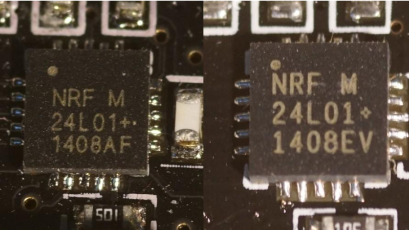
[zeptobars], the folks behind all the decapping hard work and amazing die shots are at it again. This time they decided to look under the hood of two identical looking Nordic nRF24L01+ chips.
The nRF24L01+ is a highly integrated, ultra low power (ULP) 2Mbps RF transceiver IC for the 2.4 GHz ISM (Industrial, Scientific and Medical) band. Popular, widely used and inexpensive – and the counterfeit foundries are drawn to it like honey bees to nectar. But to replicate and make it cheaper than the original, one needs to cut several corners. In this case, the fakes use 350 nm technology, compared to 250 nm in the original and have a larger die size too.
These differences mean the fakes likely have higher power usage and lower sensitivities, even though they are functionally identical. The foundry could have marked these devices as Si24R1, which is compatible with the nRF24L01 and no one would have been wiser. But the lure of higher profits was obviously too tempting. A look through Hackaday archives will dig up several posts about the work done by [zeptobars] in identifying fake semiconductors.


Fake and counterfeit chips are a real pain in the ass for anyone trying to make large quantities of low cost products
“The foundry could have marked these devices as Si24R1, which is compatible with the nRF24L01 and no one would have been wiser.”
Well, it depends on how they actually made it compatible. It still might’ve been illegal in some countries.
Also curious where the Si24R1 bit came from, as I don’t see any indication of that on the die.
I read that to indicate that they function the same but have different designation. 10s on google search results skimming abstracts implies NF24LOI is a compliance standard and Si24R1 is a chipset that meets the requirements.
So in this specific case it would be like putting store brand facial tissue in a Kleenex branded box. They do the same job but one costs more for some generally minor (but worth the extra $) differences.
I think HaD reworded tfa’s text incorrectly… Had the foundry marketed the chips as compatible, like has been done with the Si24R1, it may have been perfectly legit.
The foundries are not the one that does the packaging.
>May 12, 2009 (China Knowledge) – Intel Corp, the world’s largest chip maker, will outsource its Southbridge chips to Taiwan-based Advanced Semiconductor Engineering Inc (ASE) and will close some assembly and testing plants that are not cost-effective, sources reported.
These chips could easily been unmarked or have their labels sanded off and engraved with a cheap (Chinese) laser engraver at the back of a store. For the module that comes with a black glob on the bare die, that’s as legal as they can be.
“Popular, widely used and expensive” …Expensive? They are 1.5USD for 2.4GHz transceiver. Not sure I’d characterize that as expensive. But the challenge of counterfeits is still a big issue. The savings is one dimension but the bigger challenge I see is back-dooring transceivers. Not something I want to think about but unfortunately now I have to…in a BIG way. Especially when I think about networking my home or a hospital room or a factory somewhere. Ugh.
I think he was talking about the board it came on, not the chip itself.
One should always buy devices from an authorized distributor. Normally these are listed on the vendors website.
I’d bet mine are ALL counterfeit. Where’s my loupe?
hehe. Every one of them! I wonder if that’s why the enhanced shockburst mistakes the same packet transmitted again for a retransmitted packet and discards it.
I second this, the enhanced shock burst implementation in Si24R1 flips a single bit from the NRF24l01+ and are fully incompatible for variable sized payload use. It took me a long time to figure out why our mesh network would make two device-specific trees…
I just went through a world of pain because of the Si24R1. Wish I’d read this thread before!
At first , I had ten units of what I thought was NRF+, but after running into [tom the brat]’s issue repeatedly, I checked the tiny print which read Si24… . So I got another ten units from a different dealer on Ali, and although they’re clearly marked NRF… , they’re counterfeits! >.<
How can one know for sure at all. These guys don't exactly put up high res pics where you can compare the location of dots :p
The solution is to add one byte to the payload that's incremented each time. So now I need to implement a random number generator on my PIC16F so that it starts with a different number on each boot up. bleh!
Everytime zeptobars is posting a macro shot of a new chip I wish there were someone labeling all the areas like “that right here is a bus, these are some inductors and that must be the …”. Can please someone shine some light into what I’m looking at?
I second this.
All in favor say “Aye”.
“AYE!!!!!”
Motion carried.
The swirls are inductors. Don’t seem them very often on IC’s except for RF ( such as this obvious ). The rectilinear block on the left is all placed and routed digital logic. Hard to tell from the picture but I believe the very regular large blocks with black stripes are resistor banks. In the center section towards the top the perfect squares look like metal-metal caps probably. To the left of the swirls in the middle it’s looks like a large metal plate shield protecting something beneath.
I always wish when I see decaps for better resolution. I’m an ic layout designer so it’s fun to see other people work.
Rob
Thank you. Have a Hi-Res 346 Megabyte die shot of a S1D15719 for your work. You gonna like it.
https://twitter.com/whitequark/status/533814491314921473
(Direct link: http://fehu.whitequark.org/files/S1D15719-1.png)
(I’m sorry for image quality, my microscope setup was quite poor.)
wow! thank you! What a monster of an image!
To add to Rob’s post, The squares on the perimeter, with discolored circles, are the bondpads, for connections to the package pins. The circles are where the bond wires were etched (or pulled?) off. I don’t know what the die size is, so it is hard to estimate the bond pad size and bond wire size… but it might be around 1 mil (25um) diameter wire, or less.
The two of the widest ‘traces’ on the perimeter are likely power and gnd (VCC or VDD and GND or whatever they’re called, I didn’t look at the datasheet). These are the main power / gnd buses that get routed to the rest of the IC, and provide low impedance for ESD protection at the bond pads. The cells immediately next to these bond pads are the ESD protection devices. Could be steering diodes to power / gnd or a self contained cell that protects the pin and it circuitry from ESD zaps. You’ll notice that from pad to pad, all of the adjacent devices look the same.
At the very bottom of the first picture, you’ll see some other stuff going on down there…. Some circuits that are really close to that die. Foundries will put test structures in there to test how the devices in that process are working. Sometimes these structures will be in the street (between die) and sometimes they will be drop-ins (replacing several die in an array of x by y die). For example, say you have a standard diode and a resistor and you want to monitor the diode i-v characteristic curve (or on voltage, VD) and the resistor’s resistance for every lot. You just put these devices in there, with some bond pads for terminals, and then immediately after completing wafer fabrication, you can probe down on there with an automated prober and probe card, and electrically test that device, without all the other circuits / devices causing other variables and complications. This is done for all or most devices used in that process, in various test conditions. Wafers and / or lots are subjected to pass / fail limits based on the results of this testing, and if later on, yields are down or problems occur, you can review this data (PCM data, process control monitoring, is one term i’ve heard) for correlations to whatever problem is occurring down the chain.
This is more general IC stuff. I don’t really know RF so I can’t help with the specifics of this IC.
The Nordic transmitters limit transmission power to 0 dBm and somehow the foundries there found a way (like this) to boost the output power of the chip itself without adding extra bits.
Also recently I saw some modules going for less than 1$ (in quantities). They have the RF chip as a black blob (COB encapsulation), and I think they might be similar to this.
Typo: “expensive” should be “inexpensive”.
These differences mean the fakes likely have higher power usage and lower sensitivities, even though they are functionally identical.
Well? Do they or don’t they?
I have been waiting for a confirmation of this for a long time. In my very superficial tests, they consume more like the RFM73:
http://www.hoperf.com/upload/rf/RFM73-Datasheet-V2.0.pdf
Recently supplied 10 nRF24L01+ with gunk on chip and missing 10 smd components from China. Tests say the parts do not work which is not surprising considering the number of missing smd parts. Supplier: http://www.aliexpress.com/item/10PCS-NRF24L01-Wireless-Transceiver-Module-2-4GHz-For-AVR-ARM-Arduino-MCU/658370933.html QA is non existent with this supplier which is, of course, very costly for me.
Many moons ago…
I was working for a (large) company that had a Chinese manufacturing arm. We were building high-end instruments (range -40 +60C at stated accuracy) and parent company ordered us to send the designs to Beijing. We complied…
What a crapfest. First round was rejected-nothing says “junk” like burned PCBs and really iffy rework. Second round passed visual, but tanked at -10C. The TI ADC was the culprit.
Call to TI support “Yes, failed low temperature.” “What’s the lot number?” Number given, long pause…
“That’s not one of ours.”. GENUINE COUNTERFEIT! That was 2008. I can’t imagine things have improved.
From what I gather the way to deal with chinese manufacturing is to go there, set up the standards in the production and once all is set up and they understand what you want and you see it working it pretty much runs itself and all is OK.
But to simply call.or mail and say you want something to some specs is definitely not the way to do it, you have to go on-site. And I mean on production sire, not just in an office in china.
Of course I mean in the case of serious manufacturing, for some low cost low quantity stuff that might not be practical..
It’s a bit like teaching a kid to ride a bike, you need some presence but after you took the time and care and noticed what is done wrong and corrected it it it’ll quickly be OK. and self-sufficient.
Go there? we were already there (this was an in-house job from higher-ups that ALLEGEDLY knew what they were doing…) It’s worth noting that the fab arm didn’t even have a temperature-controlled test cell (admittedly, not cheap, ours cost Au$40K) so I guess they thought the company break-room fridge was good enough.
As far as standards?
I heard that a manufacturer (Sachs) went to china to make one of their products, the MADASS, a minimalist 49-odd cc bike that was actually well received within the motorcycle community. They did set up a factory, set standards and then walked away confident…right up to the point of a year down the road being lambasted by the bike press when the chinese bikes failed spectacularly. They are just now getting their (stuff) together-using a new “distributor” in china, which I read as “manufacturer”.
Point well received (standards and contractual adherence) but when chinese manufacturers are willing to violate international copyright law, I’d imagine standards are way down their priority list.
It’s not enough. You have to constantly monitor and check even once production is rolling. A lot of chinese manufacturers have no quals about substituting cheaper (counterfeit) parts 996 pieces into a 1 million piece run if they can earn a few extra bucks. I can highly recommend reading “Poorly made in China” by Paul Midler, who manages to show just how far manufactureres will go in a quite amusing manner.
The SE8R01 modules are dirt cheap – 40c in small qty. They don’t interoperate with the nrf though.
Wow….just when i thought the $0.9 for the NRF could not get any lower…. Any experience using them?
Very interesting. I have one NRF24L01+ module with an unusually high immunity to power supply noise – this one at least appears to have a genuine chip. At least four others required additional filtering to work reliably in the same circuit (10uF in parallel and 1ohm in serial on both VCC/GND), which I started including by default, after which I did no further testing. Of those I can readily inspect, ALL of my modules (except that one) appear to contain counterfeit chips. These were purchased over the span of more than a year, from various sources, so apparently counterfeits are very common.
I don’t know if they suffer reduced sensitivity. It hasn’t been obvious at least, but a side-by-side test specifically for that may reveal a difference. I haven’t tested power consumption either.
Plus I don’t use Enhanced Shockburst at all. To clarify, is that confirmed broken in the counterfeit NRF24L01+? And what exactly is the Si24R1? Is that just what they’re calling the counterfeits, or is it some other genuine semi-compatible chip?
Yep, every single one of my damn boards has a fake on it. This explains a bit of the wierdness I have been seeing.
So…stupid question here…how exactly do these fakes come to be? It takes considerable investment and skill to produce even the copies and so have them work at all requires a good deal of precision. Are they working from the original’s specs (i e. “Here, make one that does this, and cheap. Oh yeah, by Thursday”), or do they have schematics?
The layouts are obviously different, but at some point wouldn’t the “Make one of these, cheap” argument begin to filter into the “legit” manufacturers too? Wouldn’t there be a market for implementation of the substandard devices from any source?
Obviously I’m a hobbyist at best, but the production economics/logistics/marketing of this are really interesting.
My guess is that rather than using specific designs to specifications like the originals, the counterfeits just toss together pre-designed modules that get close enough to mostly work. Basically instead of a specific Lego set the counterfeit companies grab a handful of Mega Bloks and make something that kind of looks the same.
There’s also stolen designs.
if the clone is similar but not identical then the design could have been carried out the door in an engineer’s head
A few points:
First of all, the question whether a chip will be commercially successful is a large risk and if you can guarantee that a part will be successful, you have saved a large ‘cost.’ For cloners, they only pick the most popular, so can guarantee volumes of millions (assuming they can deliver on lower cost).
Also, IP (intellectual property) reuse is very helpful. The analog (RF) portions of a chip are difficult to verify, so if for example, you already have a design for a GFSK transmitter, changing the interface (digital portion) to follow the packet format of the nrf chip is a far more manageable task.
It would require a real company on the other end with real engineers and real experience. It is not free to reimplement chips, but very common all the same.
In this case, the most similar nrf24l01 clone is the SI24R01 (data sheet available on baidu), but there are others as well.
because it’s way cheaper to have some other company pay for marketing
because engineers quit and take their designs elsewhere, you can store chip designs in a human brain
because “stuff happens” during third shift that the boss doesn’t know about
I’d imagine the same way WE reverse-engineer items, namely to see what it does and emulate it.
For a logic chip, you set up a list of parameters using as much data as can be found (datasheets, instruction sets, etc) and then design a chip that emulates those instructions. Considering an FPGA can emulate a micro nowadays it isn’t a huge step from a set of rules to a chip that can emulate it.
RF design sparks a new set of constraints (I’ve heard dealing with high-speed logic and microwave frequencies is still practically a black art) so counterfeit designers will go with previous designs known to work. This accounts for the visual differences in the example dies in this article.
And of course is that if me amateurs can uncap an existing chip and do detailed analysis of the die using nothing more sophisticated than a few chemicals and a good camera/microscope combo (and a lot of patience and practice) that when you focus the industrial heart of a state-run enterprise at it, this is probably “all in a day’s work” for them.
So found out all mine are counterfeit, I am sure they will work for what I need. But how do you go about buying legit ones? Got mine off Amazon, figure it would be safer then ebay….
Buy from a authorized distributor. Newark, digikey, future, avnet ect.
Thanks, I will go there from now.
Another question, where do I find it in the form factor, ready to use in a prototype, not the single chip, but like the modules you can buy? I can only find on digikey the chips, not the breakout board with pins etc.
This is my question as well. Newark does list one NRF24L01+ module from Olimex, but at $32.23 (and out of stock), it’s not helpful.
I do a lot of design with the Nordic parts, both the 24L01+ and the 24LE1. I’ve bought a lot of the cheap Chinese “24L01+” modules for prototypes. They often have trouble meeting the RF specs of the Nordic parts. For example, operation at the ends of the ISM frequency band. They are also less sensitive (although, to be honest, I don’t know how much of that has to do with their PCB antenna and matching circuitry). I have always suspected they were counterfeits (or factory rejects) because of the extreme low cost.
Mine appear to all be counterfeit as well, but they work just fine for my purposes, “[Enhanced] ShockBurst” included (AFAIK just auto re-ack delay&count)… Searching for Si24R1 on AliExpress brings up everything saying “NRF24L01+ compatible” at a seemingly higher price point as the counterfeit ones I ordered
Let me start by saying that I do have a dog in this fight as I work for Nordic Semiconductor.
The re-marked nRF24L01P (+) clones are not 100% register compatible. The issue with the counterfeit devices is that when they enabled “Dynamic Payload Length” (EN_DPL) in the “FEATURE” register, one bit get’s activated in the on-air payload (the NO_ACK bit) This bit should be active high (according to the Nordic datasheet), but it’s actually implemented the other way around. When EN_DPL is activated, the NO_ACK bit get reversed in the real nRF-devices. They did such a good job of cloning they cloned the datasheet error into the device!!!
If someone is using the fake parts on both ends it will work to some degree. In a mixed environment where you may have both real L01P and the fake ones you will have issues. But don’t look to be fully “compatible” with the real nRF24L01P firmware wise. And on a side note, As the nRF24LE1 and nRF24LU1P both use the nRF24L01P radio this makes the counterfeit parts incompatible with those as well.
If anyone would like the Gerber files for the 2 layer nRF24L01P based dongle that Nordic designed they may be found on the Nordic Semiconductor website. Look under nRF24L01+ Evaluation kit then download and then nRF2401P-EK
Thanks a ton Jay for this detailed description. I’ve been struggling for a little while with these fakes http://ncrmnt.org/wp/2015/03/13/how-do-i-cost-optimize-nrf24l01/ and apparently came across the very issue. And yes, I’m (now) having a mixed environment here.
Perhaps a tester could be made with either the nRF24LU1P dongle or the nRF24LE1 or with a known, genuine nRF24L01P based module. A quick communication test could determine the status of the device / module under test.
Correction on my previous post. I stated “Look under nRF24L01+ Evaluation kit then download and then nRF2401P-EK” This should have been “nRF24L01P-EK”
This may be found under the nRF24L01+ development tools and software section then under the download tab. The hardware files for the Nordic OEM module from the Evaluation Kit are in the zip file.
JT
> Perhaps a tester could be made with either the nRF24LU1P dongle or the nRF24LE1 or with a known, genuine nRF24L01P based module.
I thought about it the instant I realized the stuff I got were COB fakes. However I counted there are at least 4 or 5 kinds of fake nrf24l01+ out in the wild. And with hell knows what differences and how many revisions.
Some come with different default pipe addresses, and work fine with genuine nrf24l01+ (In fact, since all my stock came from aliexpess I can’t b sure in anything).
all i can add here is, metoo. but i have a question, below.
i’m deploying dozens of them in various environments, some the integral PCB antenna version and some SMA connectored external antenna jobs. i get mine from Aliexpress suppliers. i did get a batch that have very odd intermittant compatibility issues (with “real” or at least “decently-compliant” clones), as well as absurdly, shockingly, bad RF sensitivity.
my protocols do autonegotiation of addresses so i don’t use auto-ack but i do heavily rely on dynamic packet length, and my bad ones always return packetsize=32.
question: can any of the incompatible ones be ID’d by setting/examining registers? i may have some of the flipped-DYNpayload chips, but can that be detected via examining registers? i’d like to build this into my driver (https://github.com/tomjennings/SR_NRF24L01). if not i may have to sit down and do side by side register comparisons and see if i can tell.
HI I bought 2 nFR24L01+ chips (local reseller I suspect he get its stock from ALiExpress or any other Banggod’s like chise web site) and guess what, one say it it is only nRF240L01 (no “+”) and whenever I set parameters nothing changes they all stay with zero value, I spent 2 hours trying to make them communicate with each other but no way as I cannot set any parameters on the bad one.
Here is side-by-side picture : http://i.imgur.com/M3bUQOA.jpg
By the way I am trying to make use an USB nRF24L01+ key the one that first show as unknown device “ia-thinker” under Windows. Once installed the .INF (declare it as usbserial device) it creates a COM port and the doc say it uses AT commands but whatever I try (including the sample from doc) no OK back ,nothing, I also tried an other one and also a FTDI USB module especially designed to plug a classical nFR24L01 module on it :-(
Hi Dodutils,
How about the nRF24LU1P? The nRF24LU1P (+) is basically the nRF24L01P with a highspeed USB 2.0 block, 32K flash and a 8051 based Microcontroller. This part is used in the majority of brand named mouse / dongle products.
As far as I know, there are no counterfeit or cloned versions of this part. The datasheets and SDK are downloadable from the Nordic website as well as the layout files for the dongle.
Maybe that device would work for your project?
BTW. There was a Nordic Semiconductor part called the NRF24L01 before the P (+) version was released. Major differences were that it did NOT have the 250Kbps on air data rate, The LNA was programmable (vs. a Fast AGC). There were other subtle differences. Using the 1Mb/s and 2Mb/s on air data rates they are “on air compatible” with each other.
They are not 100% register compatible. These parts are still shipped to some companies that have FCC certs with this older parts however the nRF24L01 is not recommended for any new designs.
~~ Jay
As I already bought the USB Key i’d like to understand why I cannot use it ;-)
It is this http://www.dipmicro.com/store/USBRF24
I have looked for a lot of relevant module manuals to check the problem, but as a novice, I still don’t understand enough. The manuals inside, https://www.feasycom.com/service/BluetoothModule.html
You linked to manuals for “Feasycom” Bluetooth modules. You are aware that the nRF24l01(+) is simply a 2.4 GHz transceiver right? It’s not bluetooth. The datasheets (manuals) can be found by searching “nrf24l01” or “nrf24l01+” or “nrf24l01P”.
Not sure how often editors look at comments, but the first link should be changed from https://zeptobars.ru to https://zeptobars.com due to the original .ru domain being blocked. Back in 2022 it was redirected, according to Wayback Archive: http://web.archive.org/web/20220601000000*/http://zeptobars.ru/en/read/Nordic-NRF24L01P-SI24R1-real-fake-copy