Laying out one PCB, sending it out to a fab, stuffing it with components, and having the whole thing actually work when you’re done is a solved problem. Doing the same thing and having it plug in to another PCB… well, that’s a bit harder. Forget about building a PCB and having it fit inside an enclosure the first time.
The usual solution to this problem is printing the board to be fabbed on a piece of paper, take some calipers, and measure very, very carefully. Extra points for sticking a few components you’re worried about to the paper before lining the mechanical prototype up to the existing board. [N8VI] over at the i3 Detroit hackerspace had a better idea – print the whole thing out on a 3D printer.
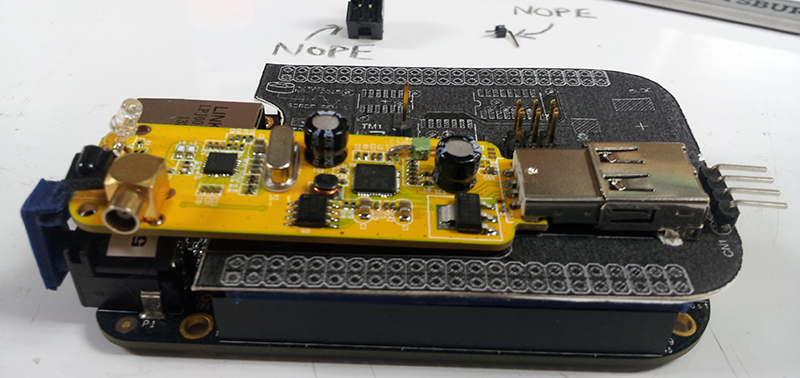
[N8VI] is working on a software defined radio cape for a BeagleBone. He was a bit concerned about a few caps getting in the way of a board stack. This was tested by printing out a bit of plastic in the shape of the new board, adding header spacers and parts that might be troublesome.
While the idea is great, there’s not much in the way of a software solution or a toolchain to make plastic copies of completed boards. We know rendering 3D objects from KiCAD is rather easy, but there aren’t many tools available for those of us who are still stuck with Eagle. If you know of a way to print populated boards, drop a note in the comments.


One could also export the PCB as a 3D model and import it in a CAD software and check for collisions with the enclosure model. I have done that in the past with Altium Designer and Solidworks.
Good to know, I am in the process of doing exactly that with the same two programs. Any problems I should be aware of?
I’m not qualified enough to know much about it, but I’m still learning PCB design and if the lack of component footprints is anything to go by, then getting accurate 3D models will be a nightmare if you need exact measurements, of course to get around that you make the 3D models but still.
One thing I have learnt is that (good) connector manufacturers have 3D CAD models. I actually have to use the 3D model to fill in the missing dimensioning in their PCB footprints or to customize footprint. e.g. I used round holes instead of square ones on my audio connector because of PCB vendor design rules.
Most of the Eagle stuff are out of date or questionable. I have issues with 2 of the Open Sourced connectors in my project – bad foot metric to imperial conversion, wrong hole sizes and locations, wrong pinouts etc. Lesson learnt.
I have seen wrong footprints and package issues in the past. These days, I do my own EagleCAD chips symbols/footprints from datasheet. Sometimes I make my own PCB, so I like to tweak a version of the footprints for spacing/width/clearance etc.
The design flow where I work involves this extensively. The first and most obvious thing to watch out for is, the model is only as accurate as you choose to make it – garbage in, garbage out. We’ve been bitten a number of times before where we cut corners on modeling the components (“Why would we ever need to know the precise dimensions? This is just a prototype, let’s not spend ten hours modeling stuff”), then six months later end up using the same model for a critical measurement and things don’t fit. Of course, all components have dimensional tolerance as well (sometimes even a uselessly wide tolerance, like 10 or 20%), so that immediately limits your possible accuracy.
At the end of the day, just know that MCAD is a nice tool, but it’s not foolproof, so leave yourself enough margin that the parts can vary in tolerance without causing problems.
We’ve done this a few times (both in CAD and printing it). One of the errors that took the most time was that the board thickness was not set correctly in Altium. Causing the final real print not to fit, as the model was thinner.
Usually board thickness is not important when doing PCB design. So the designer didn’t set it.
You can do the reverse as well, import the 3d model of the enclosure in Altium to check for fit.
I have done extensive 3D modeling using EagleUp for Eagle Cad for my HaD projects. See https://hackaday.io/project/1347-fpga-computereval-board for how closely the populate PCB is to the Sketchup model. I used it to check the PCB footprint vs its 3D model from the manufacturer and fixed a few footprints. I also used it to look at the accessibility of the layout.
Links are in my project page.
That is an awesome project! How far along is it?
“rendering 3D objects from KiCAD is rather easy”
It’s not. Components can be .wrl or .x3d, but only in a vary specific format from like one modeling package. You’re in for a real headache when you need to model your own components or use something outside the standard library. Then you can export some broken model with no materials and like half the components to try to work in your cad package. It sucks.
EagleCAD -> EagleUP -> SketchUp was a awesome before I decided to go to an open-source workflow.
This is a little too co-incidental timing… Just posted on dangerous prototypes: http://dangerousprototypes.com/2015/03/04/3d-brd-viewer-a-free-tool-to-visualize-cadsoft-eagle-pcb-designs-in-3d/
I’m currently learning/using DipTrace, which is a PCB CAD program. One of my favorite features is it’s ability to render a 3d model of the board and change the view of it in real time. I think the model can be exported in a few formats and imported into any 3d CAD program. The parts can get a bit weird. It’s a relatively new program that’s still working a few kinks out, but the primary features are there. As such, lots of through-hole parts are added to the boards with their leads uncut, and the parts are attached by the ends of the leads. This means that many through-hole parts are modeled standing on inch-tall leads. I think this wouldn’t be too hard to fix in a CAD program, and the company that makes it is probably working on the issue.
You can move the parts in any direction. I’ve do that a few times when the 3D model ‘just didn’t look right’ with an LED hovering an inch above the board
They’re all only as good as their 3d component library.
Maybe this is a little TOO accurate? Not saying this isn’t a valuable technique. But if it just barely fits using a 3D model/print/calipers/whatever, then you’ve got no wiggle room for manufacturing tolerances. Or small revisions to the parent PCB your cape will plug into. For example, the manufacturer might add some small SMD resistors/caps down the line to reduce a noise issue. Murphy’s law dictates you’ll find out about this when customers complain the metal lid on your SMD electrolytic is shorting something out on the main board, then you have a mess on your hands to fix. So if whether your caps will fit comes down to such a small measurement that it requires building a model to find out, perhaps it’s better to assume they don’t fit. Also:
“…and, since I didn’t feel like drilling 92 holes through the board, I printed the spacer parts of the two mezzanine connectors.”
Real headers could have been used just as easily. Since it’s only a mock-up, you don’t actually need 92 to drill holes – just a continuous slit for each header’s row. With a 3D printer, include the slits in the model. Or if using cardstock, just cut your slits using a utility blade, the material is compliant enough the pins will go in.
BTW also check the clearances around external connectors using actual connectors and cables etc to avoid surprises. I did the low tech laser printer out and foam. https://cdn.hackaday.io/images/1587401405632453936.png
Ah, yes, expensive mistake to learn from. Put the external connectors in CAD and the print as well. Saves you pain later on.
Really? Really? I mean, besides the time it takes to actually print ANYTHING in a 3D printer, there is the modelling effort (time spent to generate the 3D files); so is it really worth doing that? One could always take a minimum amount of care and overlook the mechanical drawings in the component´s datasheet..
Am I the only person old enough to remember prototyping on perfboard before etching a PCB? You’re not even making a working prototype, just making one to confirm physical dimensions – so gluegun smds and connectors into place, drill a few extra holes for something that doesn’t fit the grid pattern and bend over leads without solder to make components stick. The picture suggests a ten minute job using old-tech perfboard vs. ten hours to design, slice, and print a 3D prototype that most likely will be dimensionally wrong on your first attempt.
That’s so old school man… Get with the times Bubba… we have to laser cut the perfboard, then we can 3d print mock components to place on the board…
If you look at the photos or perhaps RTFA, you’ll see that the board itself is actually just printed on paper and glued to cardboard. That’s way faster than trying to squeeze it out of a nozzle. The 3d-printed parts were just the capacitor and the header spacers, then he glued those onto the paper board, along with some actual components.
He couldn’t glue the actual capacitor into place, because he didn’t have one of that shape yet — the parts-order goes in *after* the design is finalized. Crazy, right?
And if it takes you ten hours to design and print a cylinder the size of a gumdrop, you’re doing it wrong. Step out of 2011, friend, there’s better stuff now.
Printing it seems a bit extreme, I mean it would certainly gets the job done.
When I have been working on enclosures one of the first things I tend to do is make a rough mockup of the part/board I intend to go in it. Taking measurements like board thickness, hole placement and some of the larger components. Anything I think will give me trouble, smaller SMT parts (Resistors etc) tend not to be troublesome. Then it is just the simple task of making sure everything has ample room. I mean if I wanted it to fit like a glove I’d just plastidip it :P
Is this really news to anybody? Some PCB prototype manufacturers offer 3D printed PCB dummies since many years.
Am I allowed to post a link? http://www.3dcontentcentral.com (No I’m not affiliated). I get most of my parts there, and add them to my custom footprints. I stopped using ‘stock’ footprints long ago, and prefer to make each footprint (even down to 0603 resistors) myself. Tedious, but you know you can trust it. Since using 3D models as part of my workflow, I find it helps me speed up layout design. I flip between 2D and 3D in Altium all the time, I never thought it would be useful, but now I rely on it!
An SDR cape for the Beaglebone. Looks like it’s using an SDR dongle going into a USB plug.
Brad’s a friend of mine, so this isn’t straight from the horse’s mouth, but what I think he’s doing is building a doppler-RDF rig. The main purpose of the cape is to hold some buffers that drive the antenna-switcher from GPIO, and then it also seemed like a convenient place to stuff the SDR dongle itself, and then it also grew some more features…
It’s not cost-effective to redo the SDR dongle, they’re cheaper than you can buy the parts. But it’s better to fold the footprint back over the cape, versus having it hanging off the edge of the stack like a diving-board.
“Forget about building a PCB and having it fit inside an enclosure the first time.”
Why? it works out for me every single time. When the board comes back, I then adjust and print a replacement enclosure if needed. Granted I take my eagle output and run it to get a 3d model so I know what to deal with and add a MM here and there for clearance.
you can absolutely know the space dimensions your board needs before you even send the files to have it made.
I output a STEP file and give it to our Mechanical department who imports it into Inventor. We have had no issues as of yet as long as everything is modeled up correctly.
Altium designer and solid works with step files is an easy and reliable way of ensuring everything fits.
I do something similar all the time with a laser and 1/16″ thick delrin. I etch out silkscreen and pads, cut out all holes and then the PCB outline. I usually use white delrin then fill in the etchings with permanent ink. To check fit, I use actual parts and either glue them on or use doublesided tape. In about 10 minutes, I can completely verify a PCB to Chassis makeup. I even developed an alignment tool so I can etch both sides of the PCB so I can easily verify SMT parts on both sides.
I was gonna ask why not just use a laser. I bet it’s not even hard to get eagle to spit out a PDF I could drop directly in the Epilog print driver.
No PDF required. I print to my Epilog straight from GC Prevue a free gerber viewer. I also use the paid version called GC PowerPlace when I need to make some customizations. Works great for making Kapton stencils too.
I just use a 1:1 print on paper and tack it down to some foam board, as thru-hole stuff tends to be the most trouble anyway as far as layout space goes. But dropping some surface mount parts and pushing them into place with tweezers just to be sure isn’t a big deal. But you have to order all of your parts before sending the board out for fab. Probably the smart thing to do. Then I wait until I have a completed board before worrying about the enclosure. I’m not a fan of “board mount connectors lined up with slot in enclosure” type of stuff unless I was going to go into production. More trouble than it’s worth.