Atoms are small. Really small. You just won’t believe how minusculely microscopically mindbogglingly small they are. I mean you may think it’s a short way down the road to the chemist’s, but that’s just peanuts to atoms.
Atoms really are small. The atomic radius of a carbon atom is on the order of 0.1 nanometers, that’s 0.0000001 millimeters. It’s hard to grasp how fantastically small this is compared to objects we generally encounter, but as a starting point I’d recommend looking at the “Powers of Ten” video found below whose ability to convey the concept has been unrivaled since it was published in 1977.
The term nanometer might be most familiar from the semiconductor industry, and its seemingly unstoppable march to smaller feature sizes. Feature sizes currently hover somewhere around the 10 nanometer mark. So while these multi-billion dollar facilities can achieve 10nm precision it’s somewhat surprising that sub-nanometer feature size positioning, and fabrication techniques are available at relatively low cost to the hacker hobbyist.
In this article we’re going to review some of the amazing work demonstrated by hobbyists in the area of the very very small through use of cutting edge, but low cost techniques.
Nanopositioning
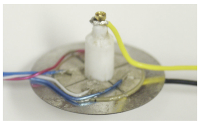
The first technique in our toolkit is sub-nanometer precision positioning. Piezoelectic materials contract in response to an applied voltage. You’ll most likely be familiar with the cheap piezo buzzers in greeting cards or beepers in cheap gadgets. However, in nanopositioning their precise motion is exploited to provide positioning. These actuators often take the form of Piezo stacks or tubes formed into XYZ stages costing of 100s to 1000s of dollars. However starting with John Alexander’s design, accurate actuators have been developed by hobbyists from cheap Piezo buzzers. Using these sub-dollar devices, cut into quadrants sub-nanometer precision motion can be achieved in X, Y and Z axis over about 10 microns of travel.
Atomically Sharp Tips

While being able to move things with atomic precision is great, it’s of little value until you have a method of fabricating nanoscale features. This turns out to be pretty simple, by simply cutting Platinum Iridium wire while pulling it using a pair of titanium wirecutters the wire can be pinched and pulled into a sharp tip. While this tip will be somewhat irregular, there will be one atom at the tip slightly ahead of all the others, providing a tiny nanoscale feature.
Atomic Scale Imaging and Measurement
Optical microscopes are limited by the wavelength of light and therefore at best provide a resolution of about 200 nanometers (2000 carbon atoms). There are a couple of neat techniques we can use however to make atomic scale measurements.
By combining nanopositioning and atomically sharp tips we can begin to build a scanning tunneling microscope (STM). These microscopes scan the tip across a surface, measuring a tunneling current flowing between the tip and the surface (in general using a trans-impedance amplifier). A version of this technique was used in IBMs famous atomic resolution movie “A Boy And His Atom”.
Hackers like John Alexander and Dan Berard have successfully built these systems for 100s of dollars. Tunneling microscopes however are limited to imaging conductive surfaces. In contrast to this, Atomic Force Microscopes exploit Van der Waals forces to deflect a tip. Because of this non-conductive materials can be imaged too, which is of particular importance in biological application. Dan has begun to work on cheap methods for exploiting this technique using affordable and effective methodology.
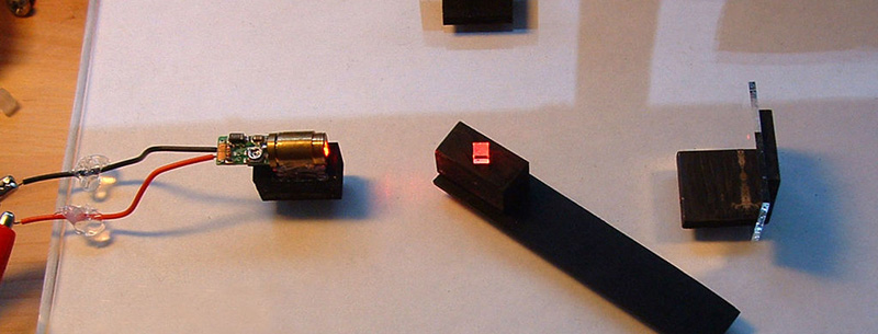
Another measurement technique which sidesteps the optical limit is laser interferometry. In this method a laser is split and reflected off two mirrors then recombined. By moving one mirror and measuring the interference between the two beams, distances can be measured. The measurement resolution of a basic interferometer will still be limited by the wavelength of visible light. However more advanced techniques (such as looping the beam back and reflecting it twice) even allow nanoscale distances to be measured. Interferometers have also been developed by hackers on a budget using BluRay laser parts and cheap laser diodes. Among other things, interferometric measurements can help calibrate, or provide feedback to Piezo actuators.
Now, with nanoscale imaging and measurement techniques in hand, what are we going to look at?
Atomically Flat, Regular Surfaces
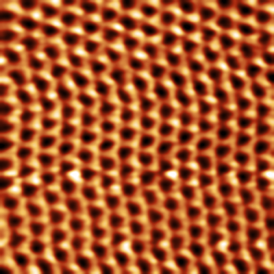
Another limitation of the scanning microscopes we’ve described is that they only work on flat surfaces. Turns out that nature has done our work for us here. Two popular materials are HOPG (Highly Ordered Pyrolytic Graphite) and Mica. Both materials are planar. An atomically flat surface can be cleaved off easily, most commonly pulled off using scotch tape! HOPG is conductive and regular. As such STMs produce great looking HOPG images. While this is interesting it its own right, we can also use these materials as a substrate. Molecules of interest can be laid out on the flat surface and imaged against a known background.
Atomically Thin Films
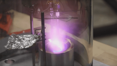
Sputtering machines can be used to apply a thin layer of material to a substrate. The technique is used extensively in the semiconductor industry to build up the layers of materials required to construct and integrated circuit. But we’ve also seen hackers experimenting with this technique. Like Ben Krasnow’s sputtering of ITO on glass to create transparent conductive coatings. Sputtering machines require a vacuum, but this is not particularly difficult to achieve, and there’s an endless variety of coatings to experiment with.
As you’ve seen, the past few years have laid a solid foundation in cheap techniques for nanoscale measurement and fabrication. These solutions, for the most part, have all been developed by a series of industrious hackers. We hope this inspires you to further build on their work and peer into the atomic realm! We’d like to hear from you in the comments, what kind of projects do you think will be built from this framework in the coming years?




+1 for the Hitchhiker’s style intro
I’m glad I wasn’t the only person to get it!
Glad you guys got the reference! :)
I like this, shame it is flash – http://htwins.net/scale2/
That’s really nice, can see it being quite a useful tool when trying to get a rough grasp on the scale of things.
Damn, was about to post that.
Even had the name copied, ‘the scale of the universe’
You got a zero to much . . .
1m = 1m
1mm = 0.001m
1ym [mikrometer] = 0.000 001m
1nm [nanometer] = 0.000 000 001m
0.1nm = 0.000 000 000 1m
0.1nm = 0.000 000 1mm
Time to say goodbye to imperial units :-)
// John Blund
Gah! Thanks, I’ve updated the article.
@John
‘micrometer’ [BE] usually is abbreviated with ‘um’ and not ‘ym’
https://en.wikipedia.org/wiki/Micrometre
Yes, that is common but also an error.
The correct one is a greek letter, I think its called ‘my’. It looks almost like an “u” but with some extra legs on it. So ‘y’ is as wrong as an ‘u’. But at least it got one leg :-)
It’s called “mu”.
I’ll guess that it will vary with language . . .
Mu is what cows says . . .
Also, typographically approximating “μ” as “u” is not just common but unambiguous.
I’d never read any paper or post using “y” for mu, but I assumed you knew some place where it was. (I don’t know your background.) Then I realized that “y”=”μ” would be incorrect anywhere [among humans on Earth], because “y” is the prefix for “yocto-” or 10^(-24), which is almost unimaginably smaller than “micro” or 10^(-6)
1 ym = 0.000 000 000 000 000 000 000 001 meters = 0.000 000 000 000 000 001 μm
1 μm = 1,000,000,000,000,000,000 (one billion billion) or (one million million million)
Kids read this board. Let’s not teach them that “ym” EVER means “μm”.
Well, kids . . .
1um=0.000 001m
And one million million million is E [Exa] ( 10^18 )
I see what you’ve done there…
You’ve got an ‘o’ to0 few ;)
Ha ha . . . Do you mean that i should written ‘too’ instead of ‘to’?
Sorry, ym [my] error . . . :-)
(I havent speaken/written english in many years now. Im a bit rusty . . . )
I use to think that so called “advantage technology” was out of reach for the mere mortals. Truth is that even simple microphones can detect movement which is in namometer scale. With ADC reaching resolutions of 24 bits, we can observe and control the realm of the atomic scale using off the shelf parts. Making it do something useful is more challenging.
That’s absolutely true, vibrational noise is also a huge issue in nanoscale measurement which I didn’t address in the article but is an interesting topic in itself.
…not to mention static!
MEMS SoCs are perhaps the most immediate possibility. MEMS is of course a few orders of magnitudes bigger than the sub-nanometer scale we are discussing here, but it seems unlikely that we are going to make a leap straight past MEMS. – Perhaps it will provide the logistics for the nanoscale stuff.
Devices such as laser pincers might also be handy here. Related to this, we have optical computing which is approaching the terahertz gap with these new vacuum transistors we have heard about. This is the range of far-infrared to mid-infrared. – Approx. 1 mm wavelength to 1um wavelength. If we can have an optical fiber in this range, then we can build fully optical computers too. – That is light and matter interacting directly as an automaton, enabled by very high transistor switching speeds.
Constructing atomically perfect meta-materials at macroscopic scale another option. For example a single crystal of iron would have an incredible tensile strength, and a specific strength far beyond carbon fibers and zylon. Kilometer-long carbon or boron nanotubes is of course tempting too.
…A few ideas!
“However more advanced techniques (such as looping the beam back and reflecting it twice)” OMG, an optical pulley-system! Why’d I not see it?!
Unbelievably impossibly mind boggling small. Loved the scale video. I remember seeing one in school, which would have been before that was made in 77. It was animated and started with a boy rowing a boat. After the trip to space, we went in to a mosquito on his arm and into a red blood cell. They portrayed the electrons whizzing around the nucleus like they knew they don’t when they made the video in ’77. Man, incredible they can actually manipulate atoms these days.
Now, I’m off to dig up and repair a freeze-proof hydrant.
A classic from the National Film Board of Canada – Cosmic Zoom. https://www.nfb.ca/film/cosmic_zoom/
Piezo elements from old lighters have also been used, the crystal in these is quite large and easy to connect with conductive paint and thin wires.
Interesting, do you have a reference for that I’d love to read more.
See 4HV, I had some success with this but lost interest because the high voltage driver chips had a habit of breaking down due to reverse current.
Also worth mentioning, see http://www.chalmers.se/en/departments/fp/calendar/Pages/Graphene-for-Ion-Detector.aspx mirroring my 2011 H-a-D posts! Nice to see one of my discoveries independently verified.
Wow, atomic resolution and nanopositioning would be a fascinating hobby. I’m sure it helps to know what technology is currently available for making precision movements and measurements. A hobby like this might get you a great job one day.