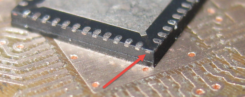
[Erich Styger] was bit by a nasty gotcha when soldering a QFN surface mount chip. The problem rears its ugly head when combining a chip possessing a padless conductor and a PCB without a solder mask. As you can see in the image above, there is a conductor exiting the side of the plastic QFN, but there is no pad associated with it. For this reason, you won’t see the conductor documented in the datasheet as a pin. It is documented in the mechanical drawing of the package, without any explicit reference to its existence. This is the Jason Bourne of package quirks.
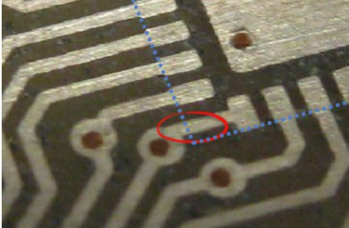 The PCB layout just happens to have a trace exiting right under this conductor. The two aren’t touching, but without solder mask, a bit of melted metal was able to mind the gap and connect the two conductors. [Eric] notes that although the non-pad isn’t documented, it’s easy to prove that it is connected to ground and was effectively pulling down the signal on that trace.
In a recent article on Hackaday I talked about “dangling pointers” and the challenge when interrupts expose the bug. [Erich’s] covered a ton of posts about embedded software. I was doing some poking around and was delighted to find that he covered the same concept and a solution for it using a program called cppcheck.


I was bit by this bug too when I was making an Arduboy business card, the capacitive touch sensor was a QFN and my drag soldering created the short.
What saved me though is before I apply power, I always like to look at each of my joints under the microscope and noticed the oddly shaped joint in the corner.
Good call. Will keep it in mind and isolate those stubs with some paintmarker prior to soldering
I’ve always used nail polish as my quick’n’cheap isolator… how is paintmarker?
Probably good, but more than the $1 I too spend on nail polish ;)
If you flipped the package over to solder it down, that padless pin would not be where you show it to be.
And if you employed your ocular globes you would see it’s mirrored on the other side :)
That’s why PCB design rules exist. If they would’ve been followed – Erich wouldn’t have this problem.
Oh? please explain?
Actually the pads are supposed to be extended beyond the package to form a fillet. You would also try to round off the other end under the package. So it would seem OP hasn’t read any of the app notes on the subject.
https://www.freescale.com/files/analog/doc/app_note/AN1902.pdf
>fillet is expected to form and should be visible on the PCB after the solder reflow
Also see the SEM picture of solder joint and cross section on page 7.
THAT is what I call a explenatory comment. very good! Indeed, the pad on the corner going at a right angle instead of extending in line can only lead to the problem above. I even make my pads as long outside the package as they are underneath to let the surplus of tin go as I have to do the soldering by hand.
Yeah, my bad. I got triggered and was too emotional to write proper comment. But yeah, rule of thumb – traces extend pads, not “intersect” them
These pads are always connected to ground. The central ground pad is connected to the plastic package shell with these attachment points. A QFN without central pad won’t have these extra pins.
I’ve seen some that say connect to VCC or NC instead of GND/NC. For example: http://www.mouser.com/ds/2/302/74HC_HCT4051_3-47304.pdf
That’s interesting. As the datasheet says, the central pad is bonded to the die substrate, which is usually at the most negative supply voltage used. Due to the way integrated circuits are manufactured there’s a whole bunch of diodes between the substrate and other parts of the circuit that need to be kept safely reverse-biased. Wonder what they’re doing to cause it to be at VCC instead.
re: gnd vs vcc substrate.
from wiki/CMOS
>The N device is manufactured on a P-type substrate while the P device is manufactured in an N-type well (n-well). A P-type substrate “tap” is connected to VSS and an N-type n-well tap is connected to VDD to prevent latchup.
https://upload.wikimedia.org/wikipedia/commons/thumb/6/62/Cmos_impurity_profile.PNG/500px-Cmos_impurity_profile.PNG
If they are using a n-substrate, the connection to the substrate is reversed to vcc.
Those are part of the lead frame. They are to anchor the center tab to the package. They do serve a purpose. They are also documented as OP has found out.
http://pkgscience.com/images/6x6_180.jpg
They would not have made contact if the pads were reflowed with the right amount of solder paste instead of being soldered by hand on a board without soldermask.
this.
I know Hackaday is all about homebrew and creative ways to do things that other people say are impossible, but a QFN that big with that big a thermal pad should ONLY be soldered using reflow and paste. If someone wants to *attempt* to hand solder, more power to them, but they really shouldn’t complain about the IC maker if they’re intentionally not doing it the right way…
Also, as pointed out in another comment, traces exiting from the pads at right angles is a no-no. Go straight out from the body and then make the turn.
Soldering these by hand is annoying but not that bad if you have a good iron and microscope. I haven’t tried it without solder mask, fortunately.
How do you do the thermal pad? I have used hot air from underneath in the past but its scetchy as hell.
Put vias under the pad and solder from the underside of the board.
thermal pad is easy, put a big blob of solder on the pcb pad, soak everyting in flux, heat it up with hotair, then put chip on top of this shitsandwitch and heat until it drops into place, push with tweezers to dislodge excess solder from under – it will create solder spheres around, remove heat while pressing, done
works great for laptop repair
I just put a small amount of solder on all pads and put the whole PCB on my vitroceramic cooktop.
And that’s why HaD warns the amateurs about it. Voilà.
My finger has been bitten by the 230V AC on similar leadframe points on the Sharp Microelectronics S216S02F Solid State Relay. Datasheet: http://www.sharpsma.com/webfm_send/321 Why would they do that?
While it does seem like a bad design, you really should not be poking around with 230V present anyways. That is just asking for trouble!
Everything exists for a purpose especially they have to go out of their way to make it.
The lead frame is like the skeleton made out of a planar sheet of metal. They placed and glue the chip on the center tab of the lead frame, wire bond the pads to the contacts before they mold the epoxy case over it. So each of the internal contacts has to supported until the molding is done.
In that photograph of the upturned chip you can just barely see the metal extending underneath the epoxy encapsulation from the large, central ground pad to the false pads on the edges of the chip.
As an engineer that has to work with electronics manufacture on this scale I’d be concerned enough about this problem to mention it to my assembly subcontractor in my design file package. It is quite possible that they would request to modify the stencil or alter the paste mixture to avoid this problem during production run builds.
Great article.
So – I’m a noob, clearly, but can someone explain to me why a chip of any sort would expose a contact like that without a pad – and a circuit board have a solder pad corresponding to that spot – and NOT have them supposed to be connected? I am going to assume there is some purpose – a test point, perhaps? But try as I might, I cannot think of one that wouldn’t cause me to roll my eyes if someone suggested it to me. What is the point of exposing a contact you do not intend to connect to (and that doesn’t appear to be an antenna or such)?
It strikes me that an exposed conductive contact that alters the behavior of the chip when voltage is applied (or ground), and has no functional purpose, is a design flaw. Call me nutty. If they have a structural purpose, maybe making them non-conductive would be a good thing…
Or maybe there’s some subtle bit of genius here that I am missing – in which case, enlighten me, please. In small words, assuming I am not a professional SMT technician. I seek to learn.
Its purpose is to hold the chip in place until the package is moulded around it. (see image above)
And they can’t do that with something non-conductive?
There is a thin layer of the *non-conductive* mold between the PCB and that extra contact. OP *solder* it to the trace by mistake. If OP had followed the guideline to extend the pad beyond the package, may be OP won’t solder that by mistake. So this is not the vendor’s fault.
Not with reasonable cost.
Metal tabs is easier to automate in process. Just lay a sheet of metal with a lot of the pad cutout, wirebond the chip, mold and cut the tabs. More in line with the process used to make the other pads (or pins).
The alternative would need to cut the pads before molding, which need precise positioning for each pad (instead of one for each sheet). Or to mold the package twice