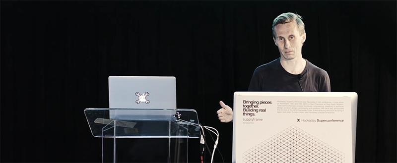
[Antti] has gained a bit of a reputation over on Hackaday.io – he has a tremendous number of FPGA projects on hackaday.io, and they’re all open source. If you’re looking for street cred with FPGAs, [Antti] has it. His Hands-on experience with FPGAs and CPLDs stretches back to the very first chips in the 70s. We’re so happy that he’s working to share this depth of knowledge, and that includes this talk he gave a few weeks ago at the Hackaday SuperConference. Take a look and then join us after the break for an overview of the FPGA terrain, then and now.
In the beginning FPGAs and CPLDs really weren’t all that great. You need only to look at the GALs and PALs of the 1970s to find the origins of FPGAs – they were single chips with a few dozen logic gates that literally needed to be burned to be programmed. Programming a PAL meant cutting a few tiny wires inside the chip with electricity, and if you knew what you were doing, you could build a chip with any series of inputs and outputs you wanted, within reason.
According to Antti, the ‘golden age’ of FPGAs was sometime around 2007, with huge devices having thousands of cells. With these chips, you could build an HDMI transceiver, make a perfect silicon copy of old microprocessors, or just about anything else you could imagine. While these FPGAs were, and still are, amazing, most designs that included an FPGA also required a fast microprocessor. This led to the current generation of FPGAs, the System on Chip, such as the Xilinx Zynq.
 The Xilinx Zynq is an FPGA, but also tucked away in this bit of metal and epoxy is an ARM Cortex-A9 processor, interfaces for DDR2 and DDR3 memory, and peripherals that include USB and Ethernet. The problem is, what do you actually build with a device like this?
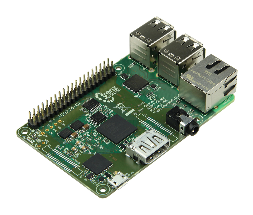
Antti has the answer to that question, and it comes in the form of a Raspberry Pi. He built the ZynqBerry, a device that doesn’t look much different from a Raspberry Pi 2. It has everything you would want – HDMI, Ethernet, and a quartet of USB ports, but this device is not built on a Broadcom System on Chip. It’s built on the Xilinx Zynq, and that means there’s an FPGA in the mix, ready to either emulate old chips, be an HDMI interface, or just there to offload computation from the ARM portion of the chip.
Right now, Antti’s ZynqBerry is the purest example of what FPGAs can do now. What does the future hold? These are devices that reconfigure on the fly. There’s a reason Intel bought Altera after all, and soon we’re going to CPUs and FPGAs combined on a single wafer that will be able to reconfigure themselves for the most powerful computing platform ever.
That’s still a few years down the line, and until then the most advanced FPGA will be the Xilinx Zynq. When the new devices come out, Antti will be busy doing what he always does: building interesting applications with FPGAs. Next time, though, it’ll be a supercomputer.


It’s Zynq, not Zinq.
The earliest programmable logic wasn’t GALs/PALs, though. It was PROMs.
It was indeed. MMI started making PROMs and then invented the technology behind the PAL.
The PAL technology was derived from the Signetics 82S100 FPLA, in production three years earlier.
Ron is correct on this. He was the designer of these chips. There are some very nice oral history interviews from the early PLD developers on the Computer History Museum we site. You can get the history from the people that actually were there.
Dang. I just read the post and caught the spelling mistake — then read the comments and noticed that I wasn’t the first.
You can blame Hackaday editorial, or you can blame Zylynx (see what I did there?) for their inconsistent spelling of their imaginary words. I think the choice is clear.
I’m guessing Xilinx got there marketing right, since no one seems to talk about the Altera Cortex A9 SoCs
I’d definitely agree with you! I had no idea Altera even made a product similar to the Zynq; the Zynq has been on my radar for quite a while.
The Cyclone V SE series. You can get a very capable dev board based on one for not huge amounts of cash. The Terasic DE0-SOC sells for $99 and has 45K LE, 1GB of SDRAM and twin A9 cores.
Yes this does read a bit like an advert. Having used both professionally, the Cyclone V is a much nicer part IMHO. It’s Xilinx’s new software (Vivado) that really lets the side down. Xilinx ISE had its quirks, but it was generally better and less buggy than Quartus II.
I happen to prefer that although they share the same die, Altera’s ARM and logic are effectively only connected via a high speed bus and each will quite happy function independently of the other, meaning more choices for optimising your toolchain.
Linux support for both Zync and Cyclone is excellent however, compared to most SoCs (Broadcom included). AFAIK, only Freescale iMX series comes anywhere close.
Can someone translate this talk into english and put some subtitles on the video?
Where can I buy on of these? I want a ZynQberry and my goal is to interface it with a few more FPGA boards! (by few I mean about 8 proper FPGAs)
It’s avaIlable to purchase at http://shop.trenz-electronic.de/en/TE0726-01-ZynqBerry-Zynq-7010-in-Raspberry-Pi-form-factor?c=188
For headless machines, you could dump the HDMI for a SATA port?
Sell me one. Hell, sell me a dozen.
Is it just me confused by the fact that this board have only 64MB of RAM? What we can dow with such small amount of ram? Is that too hard to set 512Mb (maximal avaliable RAM for 225BGA Zynq package).