We’re all familiar with semiconductor devices, and we should remember the explanation from high-school physics classes that they contain junctions between two types of semiconductor material. “N” type which in the for-schoolchildren explanation has a surplus of electrons, and “P” type which has “Holes”, or a deficit of electrons.
Unless our careers have taken us deep into the science of the semiconductor industry though that’s probably as close as we’ve come to the semiconductors themselves. To us a diode or a transistor is a neatly packaged device with handy wires. We’ve never really seen what’s inside, let alone made any real semiconductor devices ourselves.
[Hales] though has other ideas. With the dream of creating a paintable semiconductor layer for ad-hoc creation of simple diodes, he’s been experimenting with oxidising copper to make a surface of cupric oxide onto which he can make a contact for a simple diode.
What makes his experiments particularly impressive though is not merely that he’s created a working diode, albeit one with a low reverse breakdown voltage. He’s done it not in a gleaming laboratory with a full stock of chemicals and equipment, but on his bench with a candle, and drops of water. He takes us through the whole process, with full details of his semiconductor manufacture as well as his diode test rig to trace the device’s I/V curve. Well worth a read, even if you never intend to make a diode yourself.
We’ve featured a cuprous oxide diode once before here at Hackaday, albeit a rather fancier device. If this article has piqued your interests about diodes, may we direct you to this informative video on the subject?
The diode looks black, leading me to believe it’s cupric oxide and not cuprous oxide. Feel free to argue that point in the comments anyway – Ed.


The cupric oxide/cuprous oxide question from this technique came up in a thread on a metallurgy page I follow about a week ago, I wonder if it was related?
No. The original page calls it cuprous oxide, and Jenny had that in the original writeup. Hackaday commenters are extraordinarily predictable, and the cupric/cuprous argument *will* be the only thing talked about in the comments for this post.
The oxide in the picture in TFA looks black, I changed it to cupric, and that’s that. I kept the mention of cuprous for the copper pipe cap, because that looks red.
Dont hate the player, hate the game..
Or both.. I always disliked that saying.
I think Brian has both of those down
I have to admit to being an electronic engineer not a chemist, so as Brian said I just quoted the article and I bow to any commenters with the relevant chemistry qualifications to tell us what it really is.
As a retired chemist and metallurgist with almost forty years working in surface finishing and corrosion analysis I can assert with some confidence that whatever conversion products are on that sample, it is unlikely that they are of one species, or that they are homogenous, or that anyone can tell by looking at it, given the process being used. Yes color will give you a rough idea, but unless the conversion happens under controlled conditions, that’s all it is.
Could having a non-homog mix of the oxides be any better than pure forms of either?
Do you have any techniques that spring to your mind for growing copper oxides? I’d like to find out about as many as I can so I can try them.
Any chance you could reliably create the red oxide using a laser cutter/engraver?
I thought there might be some confusion: some sources I read seemed to contradict cupric vs cuprous. I’ll add some comments to the original page about it too.
I’ve given up on trying to sort out the word endings. it’s even worse for Nitrogen (my particular interest), which has 11 different oxides and ions.
Use the Stock system, which puts the oxidation state in parentheses after the element.
Copper(I) oxide, copper(II) oxide, and so on.
https://en.wikipedia.org/wiki/Stock_nomenclature
Ya that’s the convention I prefer too,
viralhog ?
sorry wrong post
Nice!, but you should also really try to make copper-oxide-ish-stuff with electrolysis. Just use two copper pieces in a solution of kitchen salt (NaCl and amount does not matter) put 5V or something on it (not too high), let it run for 1min and switch polarity, you will get a black coating on one copper electrode. Try to use this as a diode. :)
Thanks John, I’m going to try that.
When I am copper plating things, in a solution of saturated copper sulfate that has about 30 mL of sulfuric acid added too it if I use too much current or voltage, red copper oxide forms instead of the desired metallic copper.
In electroplating it’s commonly called burning. This happens on the cathode or where you place the negative lead.
30mL H2SO4 to 500mL saturated room temperature water/copper sulfate, that is.
Oooh that is handy to know, can you control it well enough to have a masked PCB so that you only lay down the red copper oxide where you want diodes for a https://en.wikipedia.org/wiki/Diode_matrix ? I guess the back of the track is one contact so you only need to connect to the deposited face somehow.
Immediately at hand I have my previously used etchant, so I might start with that and see what happens.
(Weak hydrogen peroxide + vineger + salt + copper)
The black copper (II) oxide “cupric oxide” is not what you want. It is not a semiconductor. The red copper (I) oxide “cuprous oxide” is a semiconductor, and has the properties you need. He managed to get some copper (I) oxide growth up through the copper (II) oxide layer, and that’s why the device works. When making copper(I) oxide solar cells (for example), all of the black copper (II) oxide is removed (ideally) for best contact.
I thought about this as well, but I think you want DE-ionized water, adding NaCl just makes these species to settle on the electrodes before hydrolysis of water no? i.e. you will just electrodeposit the salt on the electrodes… I also think electrolysis of de-ionized water and careful control of the voltage should allow cuprous oxide to form without cupric oxide to form… this is just speculation though. What does DV82XL think? and would it be possible to afterwards electroform copper on top of this coprous oxide layer with copper sulfate solution, to make the second contact?
There are a few so-called red patina formulas out there if you look for them that will reliably produce a copper (I) oxide (cuprous oxide) conversion on a clean copper surface, and I would look to one of those for this application, as these processes were used to produce the film when these diodes were being made commercially.
As for your second question, you can’t deposit electrolytically on this oxide surface, and anyway one can’t plate from the copper sulfate ion.
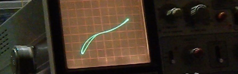
The octopus tester / curve tracer [Hales] uses in this experiment is a really useful device. More info: http://levysounddesign.blogspot.com.au/2016/04/octopus-tester-component-curve-tracer.html
I assume living in a 60Hz country wouldn’t affect performance?
no difference. In the Huntron Tracker, frequency is switchable 50Hz / 400Hz / 2kHz. It makes it easier to identify some small caps, but not really necessary.
http://www.huntron.com/products/trackers.htm
Sweet. Other than the BNC connectors for the probe inputs, I think I have everything I need in my parts bin to build one.
it is the RED part you want,
i think it will be a thin and delicate layer UNDER the black layer,
the trick is, to remove the black layer and NOT rub off the red layer
this is from memory, … i might be wrong
Copper Oxide rectifiers played a prominent part in the Poul Anderson short story “Hiding Place”. It’s a Van Rijn story, and is hard science fiction, and a mystery at the same time. Worth looking for.
That is an amazing story, 1961 and Anderson even predicted a Functional MRI fMRI like device 3 decades ahead of it’s time.
“Then this here’s a nervous-impulse tracer. It detects synaptic flows and casts a three-dimensional image into yonder crystal box, so we can see the whole nervous system functioning as a set of luminous traces.”
https://www.youtube.com/watch?v=3fNf8KX1AlQ
While you’re treating copper surfaces to make circuits, you could also use sulfur to create memristors.
http://sparkbangbuzz.com/memristor/memristor.htm
OK, if you are making them for crystal sets I found out by accident that the commutator on a small DC motor, as a result of standard use (amnd I mean small, like a phone vibrator motor) develops some kind of build up on the copper segments that makes it a diode, and not a bad one for xtal sets.
Try it.