This hacker’s video on blinking LEDs never got the recognition it deserves. At the time of writing clocking in at just 61 views, but it is indeed a work of art. Just trust me, scroll to the bottom of the article and watch it, you wont be disappointed.
Not convinced? OK, let me tell you about it and the world it has opened up in the Japanese maker scene. We’ve all blinked an LED. Maybe it was just to test a microcontroller, like the simplest Arduino example.
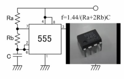
Or we’ve been a tad more old school and used the classic 555 to do it. Or maybe like me, you went through a phase of hacking together Phase Shift and other oscillators because well… it’s fun!
But [Junichi AKITA] has more extreme tastes, deciding that a custom IC layout is the way to go. [Junichi] designed a ring oscillator composed of flip-flops, then hand laid out each MOSFET placing each layer exactly where it should be fabricated.
The resulting design was then fabricated by an academic shuttle service in Japan (a bit like the well known MOSIS service). The result is a tiny circuit in the top right corner of the IC. Which of course [Junichi] then had to wirebond (check the video for a cool 1980s style Westbond machine which are still hugely popular in Japan).
[Junichi] bonded the die directly to a PCB (COB). I assume, purely for irony, a 555, and ATtiny based oscillator were also laid out on the board.
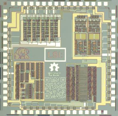 I guess you might have a couple of lingering questions. First you’ll likely bemoan your lack of your own fabrication facility (I’m still eyeing those used 1 micron fab lines that crop up on eBay from time to time). And secondly you might be asking yourself… why?
Both these questions are somewhat answers by the MakeLSI project. This growing project in Japan seems to have opened up semiconductor fabrication to all kinds of projects.
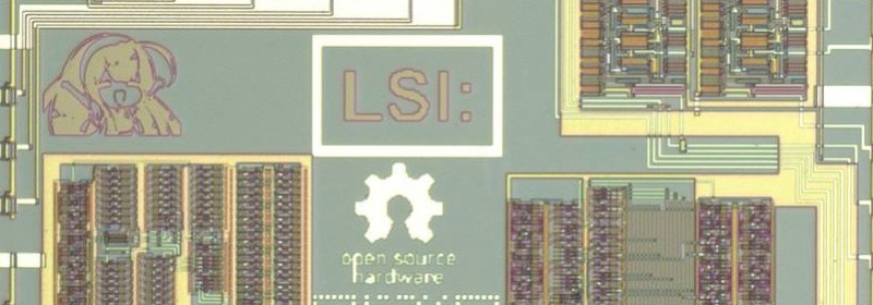
While my Japanese isn’t good enough to fully understand what’s happening it’s clear there are many awesome projects going on. Including joys such as IC layouts designed in vector graphics packages (Inkscape) and die images packed with interesting layouts, anime characters and QR codes.
For more awesome images and information (unfortunately all in Japanese) you can check them out on Facebook or on their homepage.





Best thing since sliced puppies.
The point here is not blinking an LED, it is about designing LSI at home and beeing able get it manufactured at affordable cost. I didn’t know about “the well known MOSIS service”. Now what we needs is an open source LSI CAD or maybe it exist.
There is always this.. http://web.archive.org/web/20160304120911/http://www.colorforth.com/vlsi.html
What is amazing is that apparently there have been chips designed using that software.
What I’d love to happen is older processes to become super-cheap. MOSIS is still about a 10KUSD minimum I believe. Ideally what I’d like to see is a >1micron process line with options in the 1000USD range, I feel like that should be feasible. I wonder what kinds of lines all the super-cheap power parts like regulators get made on, a MOSIS like service on those could be fascinating…
The guys at MakeLSI seem to be doing amazing work, it feels like they’ve opened up fabrication to people who want to play around. It would be great if that continues.
A batching service similar to Oshpark may be viable.
I’d love to get a standard 128 pin fully integrated template ASIC designed with a sample Chip On Board carrier.
If it proves inexpensive, than there may be some fantastic projects in the near future.
So the problem is that services like MOSIS are already batching services as I understand it, but unfortunately they’re still relatively expensive (>10KUSD). Finding a way around that would be interesting. On the other end, wirebonding isn’t they easiest of things and you’d want to find an easy way to get that done too.
“it is about designing LSI at home and beeing able get it manufactured at affordable cost.”
Yeah, and that’s amazing right? So do you not think puppies are amazing, missed my meaning? Puppies are suuuper cute, bouncy, fluffy, playful, totally awesome. Bread on the other hand, is kind of boring, mundane, (Unless you’re a revolting French peasant what ain’t not got none, but I digress) what confers it’s awesomeness as the canonical example of something that’s awesome, is the fact that it’s sliced. Best thing since sliced bread, the crowning glory of our gilded technological age, the epitome of civilization, no longer does one have to hack at a lump of food with a sharpened implement like a caveman, it’s pre-sliced! Point the kids at a butter knife, peanut butter and the bread, and worry no longer about them accidentally hacking an arm off just to get a slice. Awesomeness defined.
Logically therefore, if we apply these same benefits to something that is already super awesome, like puppies. Then we have something that is the most stupendously, unimaginably, inconceivably, hyperbolically over the top awesome thing in the whole universe of awesome ever. So like I said, best thing since sliced puppies.
Sick but so true!
SID Chips anyone?
Unlikely, the unique digital/analog design would require a manufacturing process you won’t be able to get easily…
would be interesting trying to reverse engineer a new set of masks from die shots of original chips
People did that :)
http://oms.wmhost.com/misc/
It’s good that he showed the comparison of the LSI blinker to other technologies, as you can see that the LSI version blinks much better.
A clear quality difference in both the tone and depth of blink, greater “presence”, like you’re there in person experiencing the light being on, then being off.
Precisely.
You have to have a control group/reference. LED blinking turned to eleven.
I think he won’t be truly satisfied until he has raised it off the floor with wooden spikes, and covered the top of the chip in green Sharpie.
I find the LSI blinker is slightly lacking in the richness of its duty cycle. A real metastabiliphile would have used a kiln-dried hardwood substrate, none of this PCB resin stuff.
Kiln dried?! What kind of slapdash bodger are you? Air dried…. in a Tibetan cave…. for 5.7 years.
These solid state LED blinkers just have no soul, they look artificial. I have a really awesome valve LED blinker and the blinking is much warmer and vibrant and you can really see the quality of the blink
*I had ‘joke’ tags on that comment btw but HaD seems to have eaten them
</joke>
Copy-paste this and you will get that which you desire. ;)
I think the magic word you are looking for is “warmth” of the blink.
Don’t be silly, you only get that with thermionic valve blinkers.
Thumbs up for transistor (not op-amp) based oscillators.
op-amps are transistor circuits. You can make an op-amp by wiring two transistors opposing each other. . .
Yes. But 1 transistor is better (simpler), and has more instructional value, IMO :)
Google MAGIC – it is an opensource layout tool. Only useful for the older tech but still powerful. And awkward as hell, used to require solaris! The NCSU libraries and OSU cell libraries are also opensource.
Nowadays I teach my students the Cadence Virtuoso suite but that is well north of >$100k per user per year for industry so not likely to be opensourced anytime soon. If you are in higher ed however don’t forget to talk with Patrick Haspell of Cadence who could point you in the right direction and low cost licensing.
A big shoutout for EUROPRACTICE http://www.europractice-ic.com/ who operate in Europe and handle EDA software and access to fabrication runs for higher ed/research. MOSIS also do fantastic work, without them there would probably be no/very few research or educational chips.
Magic 8.1 compiles and runs on Ubuntu 64bit just fine.
What the FOSS community needs is a good VHDL to VLSI generator work-flow that is easy to use.
I would recommend System Verilog instead of VHDL. Nearly all the EDA software vendors have abandoned VHDL and some companies are following slowly due to training lag and legacy designs while many others that started in Verilog or make large designs have made the switch.
I am not going to comment on the merits of that move (I liked VHDL), simply that all the ongoing industry research and opensource efforts (UVM, OVM) are targeting System Verilog.
Electric is still available here: http://www.staticfreesoft.com/
And there is a good “starting point for newbies” here:
http://cmosedu.com/cmos1/electric/electric.htm
So if there are 1001 flip-flops does that mean a division factor of 2^1001?
That is a silly number so I clearly don’t quite understand what is the rough switching speed of this size transistor?
Yes, each stage would divide by 2. so 2^1001. The propagation delay through T-FF’s would be a problem though, so you’d have to clock it incredibly slowly.
I understand that there are 1001 inverters, so the ring oscillator’s clock period is 2×1001 times the propagation delay of a single inverter. (I notice they also have a capacitor, which will slow things down further, but anyway.) I don’t see the number of flip-flops specified anywhere; am I missing something?
If the ring oscillator is actually running so fast as to need 2 to the 1001 to slow it down to blinky…. I’m surprised he didn’t accidentally invent the light emitting ring oscillator.
Most old chip fabrication equipment gets broken down to component bits and sold off piecemeal to surplus resellers. Some of it goes for scrap as-is while proprietary parts may either be stored for a long time in a secure company warehouse or crushed, shredded or otherwise destroyed.
If there’s any old microchip fabrication setup that is 100% complete and operational for sale, someone should jump on it like a hurricane hitting a small island. Since the investment would be far, far below what the original buyer paid for the equipment, its new owner ought to be able to do small batch IC production at prices mere demigods can afford.
What could be an issue is if the wafers would still be available. Newer production lines use larger diameter wafers and different compositions. Your shiny old late 20th century fab line will be useless if nobody makes the size and type of wafers it requires. BOLO for a complete wafer production plant to go with the chip fab.
What would be an interesting project is if some IC manufacturers would use some of their ‘obsolete’ equipment to setup a joint venture as a combination trade school and low cost short run fab for products that don’t compete with their current production.
Get a job, learn to design and manufacture microchips, get headhunted by the top companies in the industry.
IIRC 7in wafers were eol a couple of years back 10 or 11in were in, so bargain 7in stuff may not be viable long.
I’ve seen complete ~1 micron lines go for about 100KUSD. It’s not hugely common but they crop up from time to time. Smaller (2 inch) wafers are still available as there are research lines which still use them.
Don’t forget the “super dangerous” tag in this – chip fab uses chemicals that make some of the classic chemical weapons look like hand lotion. Let me introduce Hydroflouric acid for example (HF for short: http://www.sciencelab.com/msds.php?msdsId=9924296). Lovely stuff. Here is a short, anecdotal case study of a guy who was soaked in it *AND GOT TO THE SAFETY SHOWER ALMOST IMMEDIATELY* when a valve in a plant blew, http://www.sciencedirect.com/science/article/pii/S1871553207000461.
A quote or two goes a long way to make the point I feel I compelled to make:
“All he wanted to do at this point was to die; he begged his co-workers riding with him to just put him out of his misery.”
“He couldn’t see because his eyes were clamped wide open and being flushed with 1% calcium gluconate solution. A tube was thrust down his throat to flush out his lungs with 2.5% nebulized calcium gluconate.”
“he awoke in the hospital with the plant doctor standing over him, injecting shot after shot after shot of calcium gluconate to the point where he went into cardiac arrest once again.”
Note that the long term effects of many of these compounds is simply unknown. Don’t be the person who fills in the blanks in the Materials Safety Data Sheets (MSDS)!
Now I don’t say this only to shock. I am trying to say chip fab is not for the unprepared. I know this community can do it safely and properly but for everyone’s sake be respectful and careful!
Was at Defcon a few years ago, watched a talk about chip de-lidding. There I heard the greatest description of HF in its most raw form: The Devil’s Piss.
However, you can get *VERY* controlled gels of it from dentistry supplies.
Pretty rude – dropping a link that requires a subscription (whether it is paid or not) is a very unfriendly thing to do. If you want to drop a link, be decent about it and provide a real one.
My bad! It turns out that my institution has a subscription that is managed by originating IP so I didn’t even know it was paywalled.
I would post the full text but that would be illegal and I can’t find it elsewhere online, sorry. It will just have to be those quotes but if you have a question about it I could answer it (except for “can you send me the full text”).
Hi, I’m Junichi Akita, introduced in this article.
Thank you introducing my video and my project.
I’ve slightly updated the project web page contents in English (sorry not for all the contents), as well as introduction slide uploaded at SlideShare (in English!).
http://ifdl.jp/make_lsi/
There some projects to realize low-cost, short turn-around-time LSI fabrication at slightly old process, such as 1um, in Japan, whose name is Minimal Fab.
This will enable the (commercial) LSI fabrication service at a few hundred USD cost and 1-week TAT.
I believe this a revolution similar to that happened in PCB world in ten years ago.
Thanks Akita-san, your work on MakeLSI is awesome and I look forward hearing more about your progress toward a low cost fab service!
Foreign ghost white ape says your mother is a what? ;-)
Something, something, octopus…
Under 1kUSD LSI fabrication sounds awesome!
Can’t wait to see what this results in.
Hi, I’m Junichi Akita, introduced in this article.
Thank you introducing my video and my project.
I’ve slightly updated the project web page contents in English (sorry not for all the contents), as well as introduction slide uploaded at SlideShare (in English!).
http://ifdl.jp/make_lsi/
There some projects to realize low-cost, short turn-around-time LSI fabrication at slightly old process, such as 1um, in Japan, whose name is Minimal Fab.
This will enable the (commercial) LSI fabrication service at a few hundred USD cost and 1-week TAT.
I believe this would be a technology and ecosystem revolution similar to that happened in PCB world in ten years ago.
I find this fascinating, and while I understand the differences between something like a 555 timer, and a software-driven microcontroller, I am curious what would happen in something like a CPLD or FPGA.
It would simulate a similar architecture as a large ring oscillator and flip-flops, as that is mostly what the cells are comprised of. Probably a pretty large waste of resources though…
That is probably as close as I could get to this thought-experiment without buying an excessive amount of 7400’s or taking up nanotechnology to use my university’s fab equipment.
I think I have a project for this weekend…
I already knew [Junich]. Last year, he tried to do “Make LSI” (fitst time) by academic shuttle service and he got some experience.
In this year he tried to do “Make LSI” and this mask is a part of this project.
Also he want to prepare eda tool to do “Make LSI” for hobby.
I think that he will prepare eda tool to do “Make LST” for hobby.
I’m surprised the University funded and allowed such a simple project. As far as I know, only designs where some new circuit idea/topology is being silicon tested is funded
MOSIS and other fab services, I know Japan has one, allow free silicon runs in old technology for classroom, project and (in a second category) research purposes. It is in things like the ONSemi 0.5um (used to be AMI) CMOS. Bear in mind this is 0.5um 3 metal layer while someone like Intel knocks out 16nm with >10 metal layers. IBM fabs were pretty generous and MOSIS was able to offer 180nm CMOS 7RF (and now 120nm CMOS 8RF) to research.
Back in the 90s I did a chip (for the “Game Genie”) which I prototyped on an FPGA and then we hired a guy to help migrate it to a standard cell ASIC (1um). It was pretty expensive. Two things were memorable about it – one was getting to pick my own logo/text for the chip markings (surprisingly pleasing to have a tray of chips with your own made-up name on) the other was how insanely fast the chip was compared to the FPGA prototype – from what I recall (and these were early-90’s FPGAs) the ASIC was in the region of 50 – 100x faster (which we didn’t need, but was cool)
On the subject of blinking LEDs, from reading the comments, I guess none of you are old enough to remember the LM3909? It was a cool 8-pin DIP chip, whose sole purpose was to blink an LED. The neat thing was, it could do it from a single 1.5V cell (it contained some sort of charge pump to boost the voltage), and if you used an alkaline C-cell, it could do it for a whole year. If I recall correctly, the blink rate was set using a single resistor and capacitor. A lot of people built fake car alarms using these.
A chip? Bah, none of this new fangled stuff. I did it with transistors, thank you very much. Once I even made a relay blinker, which made such racket that I had to put a pillow over it. Due to the lack of any electronic literature at that time it had my own design: 5 relays turning each other on/off, like a ring counter. It was quickly pulled apart.
Ha! What a great blunder not to start with nextnano++ and simulate the transistors themselves before using them ;-)