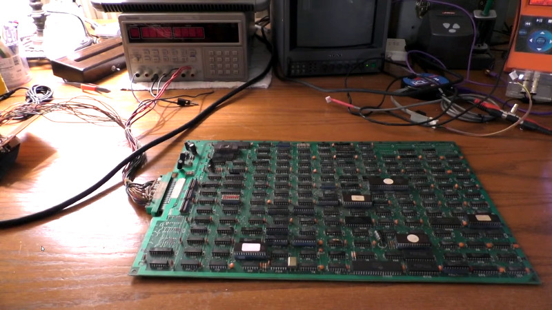
The Nintendo VS. System was a coin-op arcade system based on the Nintendo Entertainment System (NES) hardware. By being so closely related to the home console, it made it easy to port games back and forth between the two. Being an arcade system, there was significant financial incentive to pirate the boards and games, and many years later such a pirate board landed on the desk of [kevtris], who decided to reverse engineer it for our viewing pleasure.
The board in question runs Super Mario Brothers, and rather than using actual Nintendo hardware it instead relies on a standard MOS 6502 to recreate all the functions of the of the original CPU. A Z80 is pressed into service to emulate the original audio hardware, too. With much of the functionality recreated in TTL logic chips, the board is power hungry, drawing a ridiculous 3 amps when powered up. We wonder as to the fire safety of such machines all crammed into a hot, sweaty arcade of yesteryear.
[kevtris] does a great job of reverse engineering the system, even providing a full PDF schematic for the bootleg board. An old SEGA controller is hand-wired into the board to provide both game controls and act as a coin switch to allow the game to be played.
We’d love to hear the story of how these machines actually came to be, and the design process involved, but for now that may remain one for the ages. Arcade piracy was something the big companies fought against for years, with varying success – and we’ve seen arcade DRM hacked before.
[Thanks to Jero32 for the tip!]


3 amps in the good ol’ days were never a problem for that amount of TTL-chips.
I bet the 2 CPU’s together eat about 500mA.
6502 at 2MHz is guaranteed not more than 700mW -> 140mA
NMOS Z80 is guaranteed to not ever take more than 200mA. In practice both are probably half to 2/3 of those maximums.
Giant piles of 74 series logic, though? Yeah, those are very thirsty indeed.
switch it out to CMOS and you could have probably pushed it down below 1.5A but then reliability would have sunk to new and exciting lows those TTL chips were decidedly tough pieces of work especially if you went for ceramic which that board looks to primarily contain
Out of curiosity, I dug out an ancient 6502 project that I have left and measured the input current on the +5V. The board is a VERY minimal 6502 system:
6502 (NMOS version)
2732 4Kx8 EPROM
6116 2Kx8 SRAM
MC6850 UART
CMOS Oscillator/Baud Rate divider MC1440?
74LS138 1 of 8 decoder for address select generation
74LS32 Quad OR gate
74LS244 octal tri-state buffer for parallel Input
1488, 1489 RS232 level shifters
The board runs at 1.87MHz and pulls about 350mA at 5V. I did not check the +/-12V power to the level shifters. The only output on this board is the UART data, so there is no I/O current in that value.
+1 on the current comment. I used to work on arcade games back in the 1970s and 1980s, and one common failure was the nylon connector shell on the 0.156″ Molex power connectors would turn crispy brown and crack into small pieces from too much current through the power input pins. I think the pins were rated at 2 or 3 amps a piece and there were usually a couple of pins paralleled. Maybe they didn’t share current well, dunno but it was common.
Well, if one pin presents a 1mOhm resistance and the other 2mOhm, where do you think the current will go?
One third will go through 2mOhm pin, and two thirds will go through 1mOhm. Granted, BobH doesn’t say what was the total consumption, but it sounds weird nevertheless.
Additionally to the comment about current sharing:
The total resistance of the two pins:
R=1/((1/0.002)+(1/0.001))
R=0.7mOhm
Voltage across the two pins:
V=IxR…. V=3×0.0007
V=0.0021v
Heat dissipated in total between both pins:
P=IxV….. P=3×0.0021
P=0.0063W
or 6.3mW
shared between two pins:
3.15mW per pin, (can’t be asked with kirchoffs law, thus badly estimated)
My earphones can handle more than that!
.
.
Now, what will cause the connectors to begin failing is a multi-factor situation…
Many pins from back then were just tin-plated (Nickel plated if it could factor into the cost) and those tinned coatings would tarnish thus giving less surface area for direct contact to the coating from (usually spring clip) connecting terminator block and thus the resistance would increase until milliwatts became watts and that wattage had to go somewhere…
Add in the fact the cable side connectors had sprung lugs and thus had much higher resistance due to conductor quality and coating choices…
The 2mOhm connection would actually be something like a 120mOhm connection. I’d guess about 40mOhm for gold plating these days (mosfets can be around 30mOhm drain-source when fully on for the above average devices… for orange to apples comparison ).
Also depending at what voltage the 3A is at will determine if the whole board was a toasty beast or a stone cold wuss…
For example:
I assume this board is running at 5v…
P=I*V
P=5*3
P=15W
Now at 12v (unlikely… unless there are a load of regulators sharing the heat across the board):
12*3=36W
To compare the arcade board against something cramming 2 and a half times more heat in a much smaller space:
My 14inch, 16:10 ratio, 12mm thick base metal-alloy laptop can pull almost 40W maxed out (more if I were to install a core2quad), that is very noticeable when the whole case is hovering around 35*C and the CPU around 70*C with the fan screaming away (The bearings are good, it’s just heat-sink fin oscillation).
The 15W board goes in the back of a roomy (relatively to my laptop) cabinet. The only other thing to produce heat will be the display say at 200W for a CRT (and that is being nice to the CRT makers)… The 15W board usually is below the CRT in reference to gravity and thus is subject only to its own heat. Therefore the only point of fire risk is tarnishing of the connectors.
.
.
.
.
TL;DR:
pin headers waste too little heat, yet old cheap ones can tarnish and raise their resistance (and heat)
My laptop crams 2.5 times more wattage in a much smaller space and survives without bursting into flames.
The CRT in these cabinets get worse heat treatment.
I don’t know what the input current on those connectors was. My job was to repair the machines, not re-design them. As John mentions, these were cheap, tin plated connectors, that ran 18 to 24 hours a day for years on end. It is safe to assume that the pin oxidation was a part of the problem, and when one pin gets hot, it oxidizes more, raising it’s resistance, forcing other pins to carry more of the load, until the heat trashes the connector shell. I don’t have documentation on it, but I think that 1milliOhm contact resistance is an optimistic number fished out out the air. I don’t think that I ever saw a gold pin in a game machine of that era.
The power supplies on those games ran hot. Switching regulators were unheard of in that era. Some machines had a big TO3 regulator on the logic PCB and some had it on a separate power supply module. On games that had the TO3 linear regulator on the PCB, it was common to see a power resistor shunting the regulator to reduce the dissipation in the regulator. All these contributed to the board being hot and oxidizing connector pins in the power supply. Usually, they pushed 8 or 9V into these regulators and with 3 to 5A of load, that means 10 or 20 watts dissipated in the regulators alone. Later machine designs used separate power supply regulator boards to reduce the heat on the logic boards and were more complex systems as the video quality improved.
Comparisons to modern laptops have little validity to hardware of that era because of the different power supply architectures and NMOS and TTL parts consume a lot of power. In the days of TTL logic, a 4 bit counter was about as much logic as would be found in a single package. From the National Semiconductor 1976 TTL Databook, a 74LS163 pulls about 18-20mA. The smaller stuff like the quad gates pulled from 1 to 10mA each. Put 100 packages on a board and you have a few amps. In those days, you did not have a video output on your CMOS MCU, you had counters to sweep the video RAM and generate the video timing. You had Muxes or sets of tri-state buffers to allow the CPU or the video generator access to the video RAM. There is a reason that those old game PCB’s were huge.
Some of the machines were built on 2 layer PCB’s and some were built on 4 layer PCBs. Having ground and power planes in a PCB allows it to distribute heat from high power dissipation areas to cooler areas much better than the FR4 substrate of a 2 layer board. At that time, 4 layer boards were really expensive, and so heroic measures were spent to get stuff on 2 layer boards.
This goes for here on this post as well as the post on connectors and wiring. Just one word. Molex. I have cleaned a lot of those painful pins. Best is to clip ’em out and solder it up for good. Jiggle and wiggle just don’t do it.
I’m astonished that this implementation was the cost-effective approach. Nintendo could obviously keep any dedicated, arcade-only, boards under somewhat tighter wraps; but it’s hard to sell NESes to the public at even vaguely affordable prices without making genuine NES components available quite widely to anyone willing to gut an NES; while the sheer number of chips they threw at this must have kept their BoM somewhat painful even if they sold enough of the things to compensate for the initial cost of designing the emulation in the first place.
This is a clone board; the genuine one is a bit more straightforward.
Nevermind…misread your comment.
74xx series chips were cheap.
This board is about normal size for arcade.
Some boards had a second piggybacked board of the same size but that introduced reliability problems because of the connectors so they most often opted for single large boards.
What an arcade cabinet earnt was reliant on how popular the games were so game development was far more costly them hardware development.
Today a single arcade cabinet in a corner store doesn’t have to compete. Back in the day we had dedicated arcades with hundreds of cabinets. The worst one earnt next to nothing and was a net loss. The best one earnt a good percentage of total takings.
Ah man I remember the first Mortal Kombat arriving in our local arcade! And Super Street Fighter II, on sit-down cabinets with enormous projection monitors! The place must have been a money factory.
NESes were expensive back then. Maybe this design is cheaper. The Vs System also had RGB video out, suitable for arcade monitors and JAMMA. The domestic NES didn’t, and it’s video chip didn’t support it. The arcade version had differences from the base NES as well.
Even so though yes this is weird! Maybe the manufacturer had trouble getting the right chips? Particularly, in China, game consoles have been hard to sell. There’s some sort of law that prevents selling consoles with interchangable software cartridges. Only machines with built-in, irremovable games are acceptable. I don’t know why, maybe something to do with preventing samizdat-type cartridges being manufactured under their paranoid communist utopia.
Even in the 1990s the Chinese version of the N64, the Ique, had only built-in games. I dunno if that law has since changed, since optical disks replaced ROM carts.
With China having electronics manufacturing capacity even back in the 1980s, and their utter incomprehension of the principle of copyright, that would seem to be the likely explanation. Maybe it’s a fake, bootleg board, or maybe what passed for “legit” within Chinese arcades. If they had them.
Nintendo didn’t support the JAMMA standard, they used their own proprietary designs. This includes the monitor!
Ah okay. But still, the Vs System is the only source of NES graphic chips with RGB out. Which is why people will pay a fortune for them online nowadays.
The fact you couldn’t get them anywhere else, and that arcade / JAMMA monitors (ie in bootleg cabs) use RGB, means these pirates had to improvise. A standard NES graphics chip wouldn’t do RGB. Nintendo wouldn’t sell the RGB chips separately. So to produce a copy, you’d have to buy a legit one first and steal the components!
What a PIA that monitor was too. It was my very first cap kit install, and my first monitor cathode discharge. Coincidentally it was also my first arcade machine, and also a Mario Bros. to boot. It still works too. Sadly it doesn’t get played anymore.
“We’d love to hear the story of how these machines actually came to be, and the design process involved, but for now that may remain one for the ages. ”
People will do ANYTHING for money.
Nice to see Kev is still around. Almost 20 years ago when US version of Earthbound proto for NES was found and dumped, he provided some info on how to make working NES cart using compatible donor board (like Base Wars) and wire up 2x 2Mbit EPROMs.
I think that was at the height of USENET golden era,
Ah wow I didn’t realise it was Kevtris! RGVC, the golden age!
Very very cool read. I love this kinda stuff :)