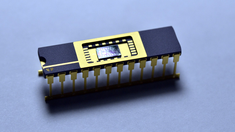
A few days ago we brought you news of [Sam Zeloof]’s amazing achievement, of creating the first home-made lithographically produced integrated circuit. It was a modest enough design in a simple pair of differential amplifiers and all we had to go on was a Twitter announcement, but it promised a more complete write-up to follow. We’re pleased to note that the write-up has arrived, and we can have a look at some of the details of just how he managed to produce an IC in his garage. He’s even given it a part number, the Zeloof Z1.
For ease of manufacture he’s opted for a PMOS process, and he is using four masks which he lists as the active/doped area, gate oxide, contact window, and top metal. He takes us through 66 different processes that he performs over the twelve hours of a full production run, with comprehensive descriptions that make for a fascinating run-down of semiconductor manufacture for those of us who will never build a chip of our own but are still interested to learn how it is done. The chip’s oblong dimensions are dictated by the constraints of an off-the-shelf Kyocera ceramic chip carrier, though without a wire bonding machine he’s unable to do any more than test it with probes.
You can read our reporting of his first announcement, but don’t go away thinking that will be all. We’re certain [Sam] will be back with more devices, and can’t wait to see the Z2.


Hey good post congrats, enjoy these types of experiences and how to
overcome various difficulties and whats need to improve chance
of positive outcomes. So I like his phrase:-
“..but is largely dependent on my coffee intake that day.”
as I have a similar issue with coffee and one of the odd side-effects
with my own mineral supplements is it now only takes one 3 shot
coffee to get me as hyper as 3 used to.
If only I had more time to investigate the chemistry of coffee and the
mineral complexes I’m dosed up on – heady complex stuff I can go
to sleep by…
But, I’m now enthused as to how one could craft a continuous process
from a suitable silicon substrate and produce heavy as in thick circuits
perhaps suited best to power products like MosFets and skip any wire
bonding to pressure pad like encapsulation.
I’ll be looking around over w/end for tidbits around this project and congrats
for starting this off as I’m sure it shouldn’t be as hard as some co’s imply.
Thanks
Speaking of mosfets, how about a microcontroller to directly switch nixies?
Hi
In University I developed a technique to use unpackaged silicon, if anyone is interested I could have a look and see if I can dig up the paper so that we could put home brew chips like this to use
Cheers
Indeed thanks Andrew re Unpackaged Silicon and with “face to face”
pressure encapsulated bonding should be able to end up with something
like a square inch of silicon die with gate electrode between highest
performing aluminium based “siliconised high thermal sapphire” package.
I’m guessing the trick is how to cement to layers in a continuous process
so any dopant migration is minimised or rather not affecting functionality.
All speculative stuff but, isnt imagination the basis of design which when
pursued with experiment is a path to an finely tuned engineering outcome ;-)
Cheers
The guts of the idea I proved was thus, using conductive epoxy you can stick wires to the die, then once that’s set you can stick them to the PCB, it all works pretty well and is largely at a scale you can do by hand under a microscope. A short spool of gold wire is suprising cheap some 20 dollars or so at the time
Tips,
-cut the wire up before you start, you’ll have no luck once you’ve bonded it
-make thimbles from laytex gloves so the wire doesn’t stick to you
-draw the smallest droplet of epoxy you can on the end of a bit of wire
-lay the wire sideways across the pad on the silicon so it sits on the ic and the PCB then walk away, come back once it’s curer and repeat till the ic is bonded
-you can then tie your inchish long lengths of wire to your PCB with more conductive epoxy
Warnings
-the epoxy does not come off silicon or gaas if you get it on the ic, sadly just give up and get annother chip
-a micro manipulator doesn’t really help, you tend to rip the wire off the silicon disconnecting it
Contender for best hack of the year.
^ This, as much respect as i have for the many people doing all sorts of great projects on had.io, this guy is a whole different league.
Someone needs to donate a wire bonding station to that man! Hero of the first order.
and also some gold would be nice :)
Sure alfcoder and if only Silver wasn’t so predisposed to dendritic
moves we could use that – well if we then accept non ROHS compliance
and at a minor level too with a bit of lead then no problemo with the
advantage silver has less resistivity than gold. My limited understanding
is the appropriate isotope of Silver with that of the ‘right’ isotope of
lead with an unusual dopant effectively halts Silver dendrites and if
we perchance dissolve the whole mass in a litre of water we still get
below the number of mg of lead for drinking water – interesting problem,
there are two metals which come to mind but, hey nuff said. This approach
overall and from many perspectives has much to offer for the enthusiastic
hacker who can adapt to any number of tech equipment when materials
tech is foremost for semiconductor properties…
Cheers
You can use copper bound wires for things that the resistance is not a big issue. Pretty much anything that is not RF related you can use copper just fine. Big companies do it all the time. I have a few samples from ST of a few before production run that are bounded with copper wires. I actually talked to the engineers about it because I was interested if they use copper all the time and the answer was they always use copper first to test small runs and change if needed. This was there MCU department.
what were the micros?
Stm32 line. NDA sorry mate.
I’m crossing my fingers that someone with a dumpster rescue manual wire bonder is reading this…
outback computers or something around San Jose.
There was an article on Slashdot, Soylent, or HAD about a place closing up shop and its inventory getting rolling into another company dealing in used merchandise in SV. The surviving company’s website had all sorts of chip and media fabrication equipment, including a few wire bonding machines. I can’t find a link now, but if someone else remembers the story or business name, maybe some crowdfunding could get the wirebonding equipment necessary to bond this prototype chip, and provide a baseline for future attempts to build a low budget home-buildable alternative to the old and expensive wire bonding machines of yore.
My thoughts exactly, anyone willing to put this much effort into this kind of project has earned NSA support in their project.
Heh, NSA support.
Since speed really isn’t the issue with this kind of project, I wonder if E-beam lithography wouldn’t be better?
https://en.wikipedia.org/wiki/Electron-beam_lithography
One of these perhaps -> https://www.ebay.com/itm/Kulicke-Soffa-1470-3-Automatic-Wedge-Bonder-Wire-Bonding/232086365188?hash=item36096ce404:g:AsoAAOSw8gVX3fj6
“He takes us through 66 different processes that he performs over the twelve hours of a full production run, with comprehensive descriptions that make for a fascinating run-down of semiconductor manufacture for those of us who will never build a chip of our own but are still interested to learn how it is done.”
Something to give the open-hardware movement some perspective.