If you’re looking to get started in designing a few PCBs, you could use one of the many software packages that allow you to create a PCB quickly, easily, and with a minimum amount of fuss. You could also use Fritzing.
Fritzing is terribad and you shouldn’t use it, but that doesn’t mean you still can’t abuse Fritzing to make it do what you want. [Arduino Enigma] recently posted a tutorial on how to design custom PCB shapes for Fritzing. Yes, Fritzing is no longer limited to rectangular PCBs with sharp corners. You can make PCBs in any shape with Fritzing, provided you spend a few hours futzing about with Inkscape.
The goal for this project was to create a rectangular board without any sharp corners for [Arduino Enigma]’s Sinclair Scientific Calculator Emulator. Fritzing can make a board in the shape of a rectangle, in fact, that’s all it can do, but [Arduino Enigma] wanted a rectangle with radiused corners. After hours of work, we have the writeup on how to do it.
The process to create a custom-shaped board, in this case, a rectangle with a 3mm radius on the corners, is simple. First, draw a rectangle of the desired shape, then draw even more rectangles as a sublayer of the current layer. Fritzing requires the layer ID to be named ‘board’, ‘silkscreen’ and ‘silkscreen0’, but this cannot be changed in Inkscape itself — you’ll need to edit the file with a text editor. After creating three layers, each containing the shape you want, simply trim the size of the page to the size of the board. Save the file, edit the file in a text editor, and click save. Launch Fritzing, load an image file, and select the SVG you’ve been working on. In just twenty or thirty quick steps, you too can import any shape you can imagine into Fritzing.
There is one pain point to this process. Editing the layer name manually with a text editor pushes this Fritzing hack from a baroque workaround into something that makes us all question the state of Open Source standards. Unfortunately, this is required because Inkscape does not use layer names as the ID in an SVG file. No, it doesn’t make sense, but that’s just the way it is.
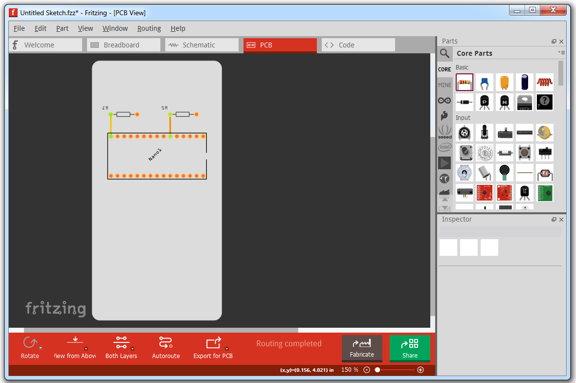
For any other PCB design tool, creating a custom-shaped board is simply a matter of drawing a few lines. Fritzing is different, though. The top copper layer is represented as orange, and the bottom copper layer is yellow, a UI decision that doesn’t make sense, even if you aren’t colorblind. Putting more than two layers of copper on a Fritzing board is impossible. Fritzing is a tool you should avoid for PCB layout. That said, [Arduino Enigma] figured out how to do something in Fritzing that you’re not supposed to be able to do and that’s pretty cool.


I just designed my first PCB this year, and am not ashamed to admit I started with Fritzing, since I was already comfortable using it for other purposes. (I’ve since started using Eagle, which has its own plethora of issues) WRTO custom PCB shapes using Fritzing/Inkscape, you CAN edit the Layer ID from within Inkscape via the XML Editor option (on the Edit menu). I was able to successfully make custom shaped boards this way without manually editing the SVG file.
One can use the Object Properties (unless layer id is some custom attribute) both id, name and etc can be changed here.
“Fritzing is a tool you should avoid for PCB design”
I disagree. It is a perfect tool for 99% of print designs
If you have never used anything else.
If you have, it feels like using a sledge hammer to repair a watch.
I disagree.
The author seems to have made a perfect board! Completely described a very standard and normal learning curve working itself into SUCCESS.
Fritzing is great for PCB work! Like any tool there is a learning curve, but hey… they ALL do. Fritzing, I’ve found, CAN BE TRUSTED. Completely!
Biomed: “Fritzing is great for PCB work!”… Hrm. But…
Brian: “Putting more than two layers of copper on a Fritzing board is impossible.”
Yeah, that sounds really Great(!), alright. Not like a limitation at all. Until you need 4 layers. But, hey, you can always do two separate PCBs and glue them together yourself! That sound like a really Great! process, not a kludge at all. But, I’ll admit, sounds completely in line with the general Fritzing user experience.
anything less than 11 layers is poorly engineered – your four layers is foul, imho.
i actually totally forgot about this software
I really hope LibrePCB: https://github.com/LibrePCB/LibrePCB takes off so we can have a non-awful PCB editor.
Fritzing seems almost like it has the potential to not suck, but nobody’s really tried. The component generation process is just craptastical.
Eagle also has a relatively crappy UI, and a subscription model that makes it really suck. But I like it better than KiCad.
KiCad seems cool, but doing anything with it has all kinds of unnecessary extra steps. It still seems to be obviously multiple separate apps loosely chained together.
Which is a great design strategy under the hood, but I prefer apps to be fully integrated at the UI level.
I made a part, put it on a schematic and a PCB in about 10 minutes after getting LibrePCB to run, only referencing the manual a few times. I don’t remember experiencing any bugs or crashes, just a few missing features.
It’s got some real potential IMHO.
KiCad 5, set to be released next week, is a lot better. You can export the netlist from Eeschema to Pcbnew by just pressing F8. But yeah, LibrePCB has some really good ideas and I’m interested to see how it progresses.
Thanks for the tip! Looks like something I will likely take for a test drive at some point.
I too am a somewhat regular user of Kicad. It’s far from perfect, but has kind of grown on me. Also waiting for the 5 release.
The worst PCB layouts I’ve seen all originate from Fritzing. I know Fritzing probably isn’t to blame, but damn…
This, so much this.
The fact that you can even tell something was designed in Fritzing should be evidence enough that it’s not a good tool.
Example?
Now you’ve made me curious :)
Friends don’t let friends use Fritzing.
Not for PCB design anyway.
Is rtzing even still being developed? it’s been a long time since there has been any updates or even blog entries.
Fritzing is pretty abandoned