If you’re looking to get started in designing a few PCBs, you could use one of the many software packages that allow you to create a PCB quickly, easily, and with a minimum amount of fuss. You could also use Fritzing.
Fritzing is terribad and you shouldn’t use it, but that doesn’t mean you still can’t abuse Fritzing to make it do what you want. [Arduino Enigma] recently posted a tutorial on how to design custom PCB shapes for Fritzing. Yes, Fritzing is no longer limited to rectangular PCBs with sharp corners. You can make PCBs in any shape with Fritzing, provided you spend a few hours futzing about with Inkscape.
The goal for this project was to create a rectangular board without any sharp corners for [Arduino Enigma]’s Sinclair Scientific Calculator Emulator. Fritzing can make a board in the shape of a rectangle, in fact, that’s all it can do, but [Arduino Enigma] wanted a rectangle with radiused corners. After hours of work, we have the writeup on how to do it.
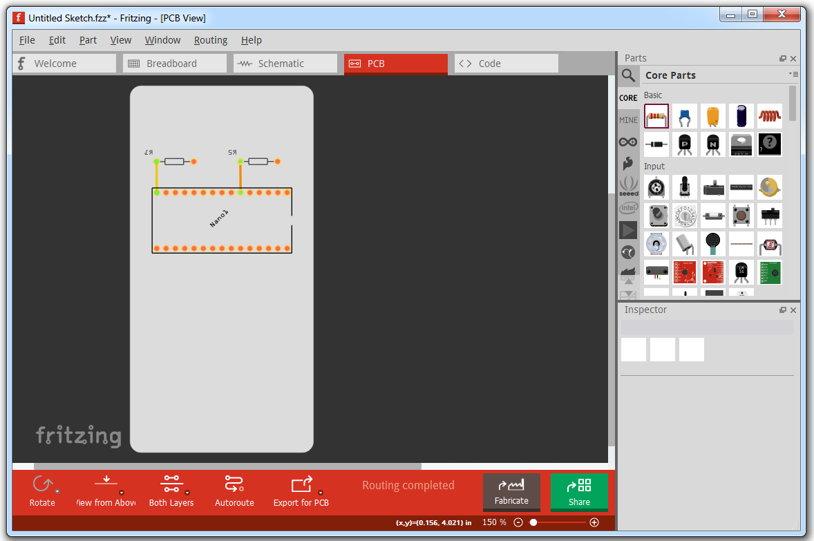
The process to create a custom-shaped board, in this case, a rectangle with a 3mm radius on the corners, is simple. First, draw a rectangle of the desired shape, then draw even more rectangles as a sublayer of the current layer. Fritzing requires the layer ID to be named ‘board’, ‘silkscreen’ and ‘silkscreen0’, but this cannot be changed in Inkscape itself — you’ll need to edit the file with a text editor. After creating three layers, each containing the shape you want, simply trim the size of the page to the size of the board. Save the file, edit the file in a text editor, and click save. Launch Fritzing, load an image file, and select the SVG you’ve been working on. In just twenty or thirty quick steps, you too can import any shape you can imagine into Fritzing.
There is one pain point to this process. Editing the layer name manually with a text editor pushes this Fritzing hack from a baroque workaround into something that makes us all question the state of Open Source standards. Unfortunately, this is required because Inkscape does not use layer names as the ID in an SVG file. No, it doesn’t make sense, but that’s just the way it is.
For any other PCB design tool, creating a custom-shaped board is simply a matter of drawing a few lines. Fritzing is different, though. The top copper layer is represented as orange, and the bottom copper layer is yellow, a UI decision that doesn’t make sense, even if you aren’t colorblind. Putting more than two layers of copper on a Fritzing board is impossible. Fritzing is a tool you should avoid for PCB layout. That said, [Arduino Enigma] figured out how to do something in Fritzing that you’re not supposed to be able to do and that’s pretty cool.


