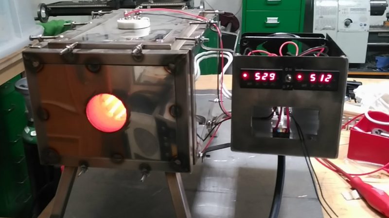
Specialized processes require specialized tools and instruments, and processes don’t get much more specialized than the making of semiconductors. There’s a huge industry devoted to making the equipment needed for semiconductor fabrication plants, but most of it is fabulously expensive and out of reach to the home gamer. Besides, where’s the fun in buying when you can build your own fab lab stuff, like this DIY tube oven?
A tube oven isn’t much more complicated than it sounds — it’s just a tube that gets hot. Really, really hot — [Nixie] is shooting for 1,200 °C. Not just any materials will do for such an oven, of course, and this one is built out of blocks of fused alumina ceramic. The cavity for the tube was machined with a hole saw and a homebrew jig that keeps everything aligned; at first we wondered why he didn’t use his lathe, but then we realized that chucking a brittle block of ceramic would probably not end well. A smaller hole saw was used to make trenches for the Kanthal heating element and the whole thing was put in a custom stainless enclosure. A second post covers the control electronics and test runs up to 1,000°C, which ends up looking a little like the Eye of Sauron.
We’ve been following [Nixie]’s home semiconductor fab buildout for a while now, starting with a sputtering rig for thin-film deposition. It’s been interesting to watch the progress, and we’re eager to see where this all leads.


“Specialized processes require specialized tools and instruments, and processes don’t get much more specialized than the making of semiconductors. There’s a huge industry devoted to making the equipment needed for semiconductor fabrication plants, but most of it is fabulously expensive and out of reach to the home gamer. ”
If it wasn’t such a niche market, I imagine costs and availability could be brought down. Designs may not scale up, but they don’t need to.
For anyone needing lower temperatures, I wrote-up rather simpler design that I use for heat-treating steel up to about 900C.
http://bodgesoc.blogspot.com/2014/11/heat-treatment-furnace.html
While I ended up just buying a kiln for glass work, I had been wondering about good methods of getting the power into it so your comment on your write-up about twisting three together is a useful nugget of information (I had been thinking of some sort of large metal terminal to change between the heating wire and copper)
If you have the ability, or drive to build one, spot welding is how it’s done in most commercial ovens.
That’s a very nice oven!
Nice Work!! Recently I was wondering if a ZVS set up in a similar configuration would be able to heat metal enough to make pattern welded steel billets. It would be much easier to cover the ends and reduce the atmosphere in something like that.
What is ZVS?
Zero Voltage Switching?
(pdf warning)
https://www.ti.com/lit/an/slua159/slua159.pdf
Well, maybe more in line with what he is talking/writing about is an ZVS induction heater,
here is one on aliexpress (I have no commercial interest in posting this)
https://www.aliexpress.com/item/ZVS-High-Frequency-Induction-Heating-Machine-for-Large-Parts-Quenching-and-Heating-Smelting-DC-Electric-Welding/32846181581.html
Diffusion dopant gasses are among the most toxic around. When things go wrong in a semiconductor diffusion process, they go really wrong. Dont kid yourself stepping (no pun intended ;) beyond simple photolithography or wet etching at a home or work shop. That said, its a really nice oven. Great engineering!
For pure Si, yes. But hackers might skip that and, as they are going to experiment anyway, go straight to SiC (carborundum) where dopants may be Nitrogen (for n) and Aluminum (for p), both rather ubiquitous elements in our environment.
It’s just that one thing, though: it is a great bit harder to cut SiC ingot into wafers than it is to cut pure Si ingots. The only thing harder than that stuff is diamond and perhaps some newly discovered artificial material made of carbon.
I’d guess lasers.
https://www.eetimes.com/document.asp?doc_id=1330333
Yup, it’s lasers.
There are spin-on dopants. There is no need to go full nanometre fab serious for very large scales.
As of now I’m working to make my first tests in 100μm feature size and I’ll be using phoosphoric acid as dopant in a Boron doped wafer.
https://twitter.com/nixie_guy/status/1019552849368412160?s=19
Hmm somehow a nice steak comes to my mind.
Tube-oven steak, lol
In my workshop I occasionally fry steaks on a red hot (bad ass torch) 15mm (~1/2″) thick stainless steel plate. If you get it right (very thin cuts of marbled meat, 5-10 seconds per side) it tastes amazing.