A few months ago, we caught wind of an interesting project in Big-O Open silicon. It’s a chip, loaded up with the great CPU cores of yore. Now, it’s finally a project on Crowd Supply. The Retro-uC project is an Open Source microcontroller for the retro geek, with a Zilog Z80, MOS 6502, and Motorola 68000 buried in the epoxy of a single QFP package. Oh yes, custom silicon and retro goodness, what more could you want?
The Retro-uC project is part of the Chips4Makers project to develop an Open Source chip for the community. Of course, this has been done before with projects like the HiFive1 and other RISC-V implementations, but really — this is a Z80, 6502 and 68k on a single chip. Let’s not bury the lede here.
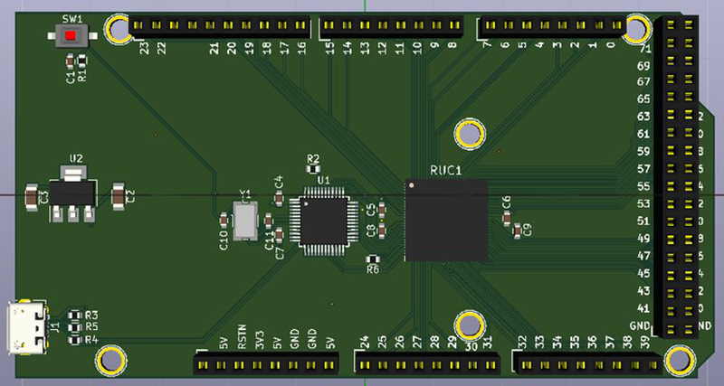
As far as the architecture and implementation of these cores go, the ‘active’ core is externally selected on reset, or can be changed through the JTAG interface. There are 72 GPIO pins that can handle 5V, with each pin mapped to the address space of the cores. So far, so good. We can make this work for some really cool stuff.
The JTAG interface is used for testing and programming, although programs can be stored on an external I2C Flash chip and booted from there. There is 4kB of on-chip RAM, and while the peripheral configuration is still being determined, there will at least be UART, I2C, and PWM peripherals. How many of each is anyone’s guess.
The Retro-uC is now a Crowd Supply project, with rewards/orders/whatever ranging from a bare Retro-uC chip for $42 USD to an Arduino Mega-ish development platform for $89, a breadboard version of the chip for $59, and a chip mounted to a Perf2+ prototyping board for $65.
While this chip hasn’t even gotten to tape-out, all the cores work on an FPGA, and there is precedent for doing Open Source, crowdfunded silicon. We’re looking at this one closely and are excited to see what everyone is going to make.
This project has been a long time in the making, with the project lead giving a talk at FOSDEM earlier this year. Now it’s finally time for the hard part of any silicon project — getting the money — and we’re looking forward to see what comes of it.


This seems cool but I’m at a loss where this would be useful.
That is what I am curious about. Last time I looked you could still get old CPU’s pretty easily and I can not see anybody using one in anything new that is going to be popular. Cool in that you can do it, but with that brain power might be better spent moving forward, but everybody needs a fun and challenging diversion. Perhaps this is his.
Most of the chips listed are still in production in some form or another and available for very little money. $42 for one of these chips, OUCH!
Maybe for some retro, as close to the real deal as possible, hardware unit that can act like multiple classic computers/consoles? Without emulation artifacts?
The thing is… FPGA’s can already do the CPU part, pretty much exactly as that is in the digital domain, the hard part is the peripheral chips like SID , analog video chips etc… anything analog really is hard to get right.
There’s some concerns there on making sure you’re voltage-tolerant, as lots of old hardware is 5V which will blow up modern FPGAs. So there is some advantage to that here. But that’s super-minor, as voltage translation isn’t that complicated.
Even then, voltage conversion is easy to do on an FPGA that has enough pins. Internal to the microcontroller, the in, out, and direction buses are all separate, so it’s easy to connect each bus to FPGA pins, then read from a voltage-tolerant buffer and write to a higher-voltage tri-state buffer.
Like this, it’s very good, but ppl still complain about video glitches and oddities… https://amigastore.eu/en/318-mist-fpga-computer.html
Whoopie
I hope there is some unmentioned advantage to using this such as increased clock speed not found in current silicon. The Amiga Vampire accelerator uses the M68K Apollo core which is 68K clocked to 3x the performance of the fastest 68060 CPU. If that is the case he’ll sell a bunch to Amiga/ST hackers.
It seems to be a plain 68k… you could run it at 4x the clocks speeds on the Vampire accelerator and it would still probably be slower. Note a 68k has an instruction per cycle rate of 0.25 … the vampire accelerator does 4 peak, probably averages 2-3 instructions per cycle.
I have no problems with Arduino as the simple HAL that lets folks get things done easily but Arduino as the oversized gaptoothed header layout is dreadfully tedious and should go away.
why not release a hacker board in the most hacker friendly format which is the gumstick , solid single row of headers in 0.1 dip spacing.
Amen. I wish people would stop reanimating that gapped layout. Its perpetrator has apologized, let it die already.
Gumstix is great. I love the Cypress PSOC dev kits for this reason, they’re a splendid example of a friendly dev board layout. Everything’s labeled, the USB adapter snaps off, etc. All the Pro Mini and Teensy products do it too, and I think they’re all the same width, even.
Did you look at the Retro-uC BreadBoard pledge on the crowdfunding site ? I think this is what you are looking for.
There are several unknown points:
1) Only a 4KBytes SRAM as internal memory, that’s extremely poor – especially if there is no way to address an external memory with the usual bus found in genuine microprocessors like Z80, 6502 and 68000.
2) C64? wait, you need a 6510, not a 6502.
3) There is no mention of a parallel io/memory bus to be able to connect to an external ROM/RAM. Does it mean there is no way to do so? It totally destroys the purpose of such chip.
4) Only one active core. I fail to understand the purpose to have three cores because they are not cheap.
5) There is no mention of the maximal frequency those cores can reach.
My opinion is the description of this chip is very poorly done and the essentials to make it attractive really lack.
Isn’t a 6510 just a 6502 with a bit of extra hardware squeezed on? Since Commodore owned MOS Tech anyway, so it saved them a couple of pence to put some of the machine’s custom hardware on the CPU. Ah I looked it up. a 6-bit I/O port. So you could do that, I would bet, either with a plain 6502 and a bit of address decoding, or maybe they’ll add it as an option to this thing.
Have to agree with others, though. Who would ever need this? You could just buy all three separately for less. When did anyone ever need the ability to switch CPU cores? And only on reset.
Is this one of those things where somebody had a bright idea and nobody stopped them? Surely there’s no market crying out for it. Strange and a bit sad.
And yep if it doesn’t actually expose the bus pins, then WTF!? There are other microcontrollers about, and they’ve had the advantage of however many years of evolution, and wide support. Just WHY would you need 3 obsolete cores like this, in one chip? If you really wanted to do some multiple-hardware emulator thing you’d just use an FPGA for the whole machine.
Originally I planned to have a different chip for each core but combining them on one decreased the cost as some of the startup costs are shared. Also it makes the logisitcs easier.
I guess everybody is different and some people love these obsolete/Retro instruction sets.
Yah it kinda sounds like you’re better off with any random FPGA dev board… not sure if that’s true or the write up sucks.
Indeed super interesting and a lot of its usefulness I think is in the learn process and experimenting better with those shared silicon projects.
I wonder, if a proper OSH Park silicon style is affordable, how could one use, in the same affordable price, the tools for designing it. Free chip manufacturing, but then 200k€ for a Cadence tool, does not sound that much cheap. Even for start-ups.
Any clue on that?
One purpose of the Retro-uC project is to do the development with open source software so other people could then later build on this project for their own custom silicon with their own blend of peripherals, cores or other things.
Ok, this is very interesting. But open-source software for syntesis (which I know exist something from Lattice ICE40 stuff)..I am not fully in this field, but layouting? Place and route stuff? What about analog design and simulation?
I have to dig a bit more apparently, thank you.
Next to the talk mentioned in the article I had another talk on FOSDEM on the toolchain: https://www.youtube.com/watch?v=ULHdrbghF2M
I like it. More info, more RAM, lower price please.
May also add that the project has a [hackaday.io project page](https://hackaday.io/project/27091-chips4makers-pilot-retro-uc)
Hi Staf, I think it would be great if you could also provide the maker community with a writeup on the whole process of how to design and then have an IC fabbed. Even if it means that very few people will do the same given the high capital needed, it would still help demistify the process to the lucky few who are able to. Perhaps this could lead to a trend of more open integrated circuit design, where people open up silicon design to allow other designers to import it into their own projects, allowing for faster iteration as the current open source software community allows.
That was always the planning. If you follow the updates on the crowdfunding campaign or on hackaday.io you will keep up to date with the progress I am making.
Hey, it is the first time I get some RTL code I wrote going into a real ASIC, sweet ! (I helped Alexander optimizing the ALU of the 68000).
Since the ao68000 is microcode based (like the real stuff) so is the 6502 and Z80.
It would be nice to have only one core and a downloadable microcode to run the 3 CPU flavors.
To answer the question about performance, IIRC, the ao68000 has a 32-bit ALU and a pretty good fmax, its performance on an FPGA is close to a 68030 @ 50 MHz. Expect more on a real ASIC.
The T65 and T80 RTL code implementing resp. the 6502 and Z80 are not microcoded.
In order the get the startup cost low enough for the low volume for the Retro-uC older technology (0.35um) is used for production. 50MHz clock frequency won’t be reachable I do hope to reach above 10MHz but definitive values I should have before the campaign ends.
If I would use smaller technologies the funding goal would be an order of magnitude higher. You can look at the unsuccessful Open-V crowdsupply campaign to see what I mean.
There was HiFive1 which was a successful crowdsupply campaign. And the processor is really fast (320+ MHz) and more SRAM (16KBytes). I would like to contribute but considering the price vs. the limitation in speed and memory, it makes no sense to make it ASIC if an FPGA can perform better.