Reverse engineering silicon is a dark art, and when you’re just starting off it’s best to stick to the lesser incantations, curses, and hexes. Hackaday caught up with Ken Shirriff at last year’s Supercon for a chat about the chip decapping and reverse engineering scene. His suggestion is to start with an old friend: the 555 timer.
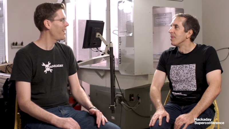
Ken is well-known for his work photographing the silicon die at the heart of an Integrated Circuit (IC) and mapping out the structures to create a schematic of the circuit. We’re looking forward to Ken’s talk in just a few weeks at the Hackaday Superconference. Get a taste of it in the interview video below.
You’ll be surprised by how easy it is to get into this hobby. Ken’s advice about taking on the 555 timer is brilliant because you can do so with a hacksaw rather than using chemicals like fuming nitric acid. Apparently if you hit eBay you can still get these chips packaged in a metal can, rather than the black epoxy that usually comes to mind. Grab a hacksaw to open the can, take a great picture of the now-exposed die, and you can start working through the structures. These chips are not built using the incredibly small scale of digital chips, and the circuits themselves are not overly complicated. Ken even has a primer that walks you through this exact process, including die photos if you want to skip the hacksaw step.
You might not make your living designing silicon, but think of this as a jigsaw puzzle for electronics engineers. You have the schematic and you just need to find where all the pieces fit.
There are many notable people working in the same field as Ken and he mentions a few of them: John McMasters at Siliconpr0n, Rob Baruch at Project 5474, and the fine folks at Zeptobars. All are great resources for learning, and getting your hands on die photos for further study.
Ken uses a method of stitching together multiple photos from his microscope using the Hugin software package. It’s the secret to die shots where every part is crystal clear, and we think it’s as remarkable as the reverse engineering work. To go deeper, check out the talk he gave at the 2016 Hackaday Superconference. We can’t wait to see what he comes up with this year!


If you’re interested in getting started, Robert Baruch has done a pretty good job with a getting started guide: https://project5474.org/index.php?title=Procedure:Techniques – he covers a lot of the chemical issues and microscopy setup.
Disclosure – he’s a friend of mine.
May as well leave my YT channel here. I have videos about decapping and reverse engineering in there: https://www.youtube.com/channel/UCBcljXmuXPok9kT_VGA3adg
Oh, also there are plenty of die photos for 74xx series chips that haven’t yet been reverse engineered here: https://project5474.org/index.php?title=Category:NotReverseEngineeredYet
http://www.righto.com
(blog of Ken Shirriff, linked here for aiding Google with its page ranking scheme. and so I can find it easier later.)
We owe a tremendous debt to Ken Shirriff for his work in reverse engineering the sinclair Scientific calculator
If you don’t care about keeping the wire bonds in place and powering up the device, plastic DIPs can be decapped without Acid. Put the PDIP lengthwise and dead bug in a vise and tighten so there is some stress in the part. Take a propane torch and heat the top of the package (i.e. underside as it is in the vise) and the tighten the vise. The die will separate from the plastic, you will get good at catching the die as it falls. Sometimes plastic residue will remain on the die so more than one device may need to be decapped this way.
Can private individuals examine the high resolution chips like an i7?
My understanding is that the scale of these, and the complexity of layers, make modern high-end chips very difficult to work with. I know Ken recommends older chips both for the ease of decapping and for the relatively large structures that are easy to capture in photos with common equipment.
An Intel i7 is going to have structures at 45 nm (1st generation ~2008) to 14 nm (5th to 9th generation ~2015 to 2018) in size.
So no, not without some expensive equipment. Visible light has a lower limit of ~ 400 nm so structures smaller than can not be observed using visible light. The cut off for using light with high end chips would probably be around 1994 ( https://en.wikipedia.org/wiki/600_nanometer )
To observe structures smaller than 45 nm for individuals the options are limited.
Well 200 nm with optical wavelengths.
https://en.wikipedia.org/wiki/Optical_microscope#Limitations
For scale, the diameter of an individual silicon atom is 0.2nm. So you are talking about examine structures that are from ~200 atoms wide ( 45 nm -1st generation ~2008) to ~70 atoms wide (14 nm – 5th to 9th generation ~2015 to 2018).
Does the private individual have an electron microscope? Or is the private individual willing to pay a small amount to have the work done for him/her?
See: https://hackaday.com/2018/10/11/a-new-kid-on-the-mini-arm-block/ for instance.
With a electron microscope don’t you generally need to sputter coat the sample in gold (to prevent the buildup of static charge). Which if you are using an abrasive to slowly remove nanoscopic layers of the samples for multipole scans, would add difficulty.
Back in the 80s, I used to de-cap fused link PALs. I figured out how they were mapped and then was able to duplicate them so I could make repairs. It was actually a lot of fun.
For some pretty amazing decapping and reverse engineering/die level exploits/hail mary attempts dumping various arcade chips and other proprietary and extremely undocumented protection roms/devices check out http://caps0ff.blogspot.com/
Some of the things they have to go through to try and preserve and document these (actually rather rare) chips in order to accurately emulate them in MAME are pretty terrifying. Without their work many of these games would/will simply be gone when the last of the original hardware dies and/or battery suicides (encryption keys in volatile battery backed ram).
Watching the mame team rip out old poor simulations for stuff has been interesting. Looks like caps0ff also has a patreon.