
Sometimes you start something simple and then it just leads to a chain reaction of things. I wanted to write a post about doing state machines in Verilog and target the Lattice iCEstick board that we often use for quick FPGA projects. That led to a small problem: how do you show what’s going on inside? In this series of posts, we’ll look at building a logic analyzer into an FPGA to help debug itself, instantiating memory, and — finally — state machines.
Logic analysis is a common tool in FPGA development. If you use Altera, they have Signal Tap available that lets you build a simple logic analyzer into the FPGA that talks back to your PC. Xilinx has ChipScope which is about the same. Sometimes those tools either cost money or are limited in some way in the free versions. I have my sights set on a tool that can be used with the Lattice architecture.
Sure, you can ship data out on I/O pins and then use a regular logic analyzer to pick up the data. But that isn’t very handy. So I thought about writing a generic logic analyzer component. But before I did I decided to check to see if someone else had already done it.
Spoiler alert: they did, but I wanted something a little different so I wound up extending the program significantly. What I wound up with is a reasonably portable Verilog logic analyzer that can produce traces like this one:
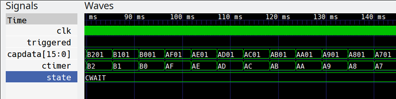
Keep in mind, this isn’t a simulation. This is real data pulled off the actual FPGA. Yes, that is gtkwave producing the plots, but the input data is a VCD file generated from samples taken inside the FPGA.
Good News and Bad News
The good news is I found the verbosely named OpenVeriFla code on OpenCores. The bad news is it was about 11 years old and didn’t seem to work right. Some of it was configuration problems on my part, but there was at least one bug that showed up if you sampled data that rapidly changed. Naturally, after I spent a few days fixing bugs, a new update showed up. So then I had to go figure out what the original author had changed and fix things up in my branch. I wound up making enough changes that I simply forked it and decided to make significant enhancements to make things more useful. However, after correspondence, the author did make a parallel change in the original to squash the same bug, so either fork should be free of the original bug that started me on this journey.
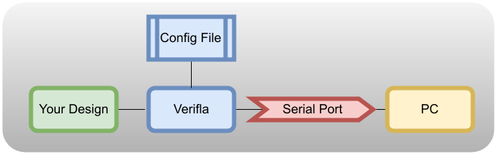
OpenVeriFla is really two parts. There’s a set of Verilog files you have to include with your project. You set the general configuration with a header file. There’s also a Java program that reads the data. This requires the flaky Java serial I/O which had some trouble finding the port on my system. Of course, the real problem will be if you use the serial port in your design — you might have to wire up a temporary serial port on an unused pair of pins just for the logic analyzer to use. In some cases, you might be able to disable your serial port just for debugging but that won’t work if your problem involves the serial port.
You’d think the Java program would display the captured data or create a VCD file that a waveform viewer could consume. But it doesn’t. It creates a Verilog model of the recorded data. You then have to simulate that model to get a VCD file. There might be sometimes that is useful, but I’ll be fixing that so you can directly generate a VCD file if you use my fork.
Not Enough Memory
The first problem I contended with was there didn’t seem to be sufficient memory on the iCEstick board to capture many samples. I suspected I knew the problem, but for the moment, I just reduced the sample size down to something very low. I didn’t want to fix the memory problem until I was certain the bug was something I wanted to spend the time to fix.
I figured if it worked for 16 samples, I could always fix the memory and add more. As I suspected, the memory component was written in such a way that the Lattice FPGA couldn’t use its onboard memory and, instead, had to build all the memory out of regular flip flops. I’ll have more to say about that later.
The configuration of the original code is all done in a file config_of_verifla.v. You can change lots of parameters, although in the original code there are a few other places things have to change. In my rewrite, as you’ll see, I changed how the configuration works a little to make things easier.
Bug Squashing
My first attempts were to simply read a toggling output line. This seemed to fail. After some investigation, I found that if a signal changed on every clock cycle, the code would miss it. It was an easy fix and the upstream made a similar fix, as well.
After that, things seemed to work OK. The configuration was a little painful and I wanted a few extra features such as a clock qualifier and outputs that show if the analyzer is armed or triggered.
There might be some other odd bugs, too. I noticed that using Icestorm, setting memory to 256 and the trigger point to 128 causes a hang up. That’s probably due to the odd memory architecture (see next section). However, using a trigger point of 127 or 129 works great.
Notes on the Original Code
The PDF file supplied with the original program is pretty instructive. The idea is you instantiate the logic analyzer core, send it the data you want to capture and use the configuration file to set things like the memory depth and the trigger condition.
There were two things that didn’t jump out at me on a first reading. For one thing, if you assert run constantly and your trigger occurs rapidly, the Java program won’t reliably find the start of the data. Unless you have a rare trigger or an external input like a push button, you will usually set run to zero. This leaves the core unarmed until the Java program sends it a command to arm it.
The other thing that is strange is how the system manages memory. Let’s say you allocate 256 words for the logic analyzer. I’m going to assume the word width is 8 bits, so those are really bytes. You can also select a repeat count width, so let’s assume that’s 8 bits, also. That means your buffer looks like this:
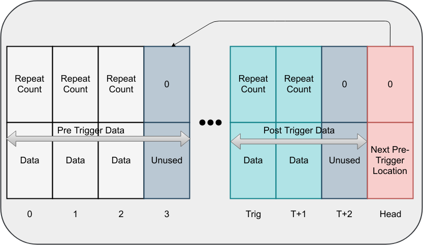
See the trigger point (Trig label along the bottom)? That’s configured in the header file, too. When something arms the block — either the run input or the software sending a command, it starts collecting data in the start of memory up to but not including the trigger point. When that memory is full, it starts treating the memory as a circular buffer. Before the trigger, it never stores data in the area at or above (numerically above) the trigger point, except that the last word is used to manage the head of the circular buffer.
When the trigger occurs, the system stores the event at the trigger position and then starts storing data using the rest of the memory. It will quit when you run out of memory or when it has read a configured maximum number of samples. This buffer is sent to the PC via a UART, beginning with the last word (FILO). That last word, by the way, won’t contain your data, so be sure to allow for that loss.
There are a few odd cases to think about here. First, if the trigger occurs before the circular buffer fills up, you’ll get blanks where nothing was recorded. You’ll see there’s a counting mechanism that will give you an indication of this, but it is still worth noting that you may waste memory depending on your configuration. In the figure above, for example, only the first three memory slots are in use when the trigger happens. Note that this doesn’t mean there were only three clock periods since some or all of the data times may have counts greater than one. If the memory fills up, the head pointer wraps around, and all the pre-trigger memory would be in use, with the oldest samples falling off as new samples are read.
In fact, the count leads to the other problem: How much memory is used after the trigger? Let’s say you have byte words and a byte-wide repeat count. To save space, the analyzer only stores samples that are different from the previous sample, as long as it can count. In other words, if you have a signal that is 00000000 for 300 clock cycles, the memory layout would be:
254 00000000
46  00000000
The count can only go to 254, in this case. A zero means no data is in that slot at all. However, suppose you have a buffer of 16 words and the trigger point is at 8. That means you have memory locations 0-15. The last one is the buffer pointer, so your data is in locations 0-14, with 0-7 being a circular buffer and 8-14 being the trigger data and the post-trigger data.
You’d think that means you can only store six samples after the trigger, right? No, because of the counting mechanism, you could potentially store a lot more. However, if you set the limit to six, and your signal changes slowly compared to the clock, you might only get the trigger with a count of six or maybe the trigger and one more sample with a count of five. Not really what you expected. In practice, I’ve found it is best to set the count to something very high and let the thing run out of memory. The only time you’d want to set an explicit count is if you have very slow signals or large repeat counts and you don’t want to spend time waiting for the memory to fill up.
Enhancements
In the end, I made nine enhancements:
- Document some of the settings a bit better
- Fix the bug where samples that changed on one clock were not handled properly
- Add synchronous memory that is easier for some tools to infer (see below)
- Minor clean ups to code
- C tool to read output and generate VCD directly (we will talk about this next time)
- Adds clock enable/qualifier (defaults to 1 so you don’t need to specify it if you don’t use it)
- Adds armed and trigger outputs
- Adds trigger qualifier (must be 1 — set by default — for internal trigger to work)
- Adds exttrig (default 0) if you want your own trigger logic
Two things to note. First, the exttrig input does not respect the trigger qualifier. I assumed if you wanted to qualify the trigger you’d do it in your own logic. Second, for proper operation, many of these inputs need a default setting. In most Verilog tools you can set a default on an input, but at least Intel Quartus does not seem to be able to do this, even in System Verilog mode. If you are using a tool like that you may have to use top_of_verilfa_nodef.v and then be sure to set the right defaults when you instantiate the analyzer.
Houston, We Need More Memory
Once I had things working reasonably well, I looked to see why the memory was so limited. To understand why it helps to know a little about how Verilog works behind the scenes.
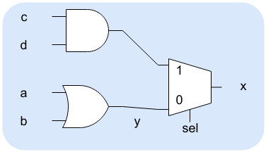
In a C program, the compiler can look at a line of code and — generally — create some machine language that corresponds to the code. In some cases, this is true of Verilog as well. Some lines of code turn into pretty straightforward logic gates. For example,
assign y=a|b;
assign x=sel?c&d:y;
Both of these statements will generate a few simple logic gates. The second one will actually generate a mux. In reality, depending on the FPGA architecture, the whole thing will likely turn into a look up table, anyway.
However, Verilog has to peek around sometimes to figure out what you are trying to get at. For example:
always @(posedge clk or negedge reset)
begin
   if (~reset) q<=1'b0; else q<=d;
end
The synthesis tool should realize this is a D flip flop with an asynchronous reset. Even if the logic is a bit more complicated (say, q<=d^inv4|force, for example), it should realize that it is a D flip flop at the core and not try to build some custom logic. We say the compiler inferred a D flip flop. On the other hand, if you said:
always @(posedge clk)
begin
  q<=d;
  if (~reset) q<=1'b0;
end
That infers a D flip flop with synchronous reset.
In the original code, the memory module implied a dual port RAM with asynchronous read capability. That is, the RAM simply presented the contents of the addressed cell at all times, not in step with a clock. Some FPGAs can model that, but the Lattice chip I was using could not. The synthesis tool, Yosys, knew that so it created the memory out of flip flops instead.
Great, right? Well, the problem is, the chip has a good bit of dedicated memory onboard that you can use, but flip flops are in high demand and eat up logic cells meant to do more complex tasks. That’s why I could hardly get any memory.
The answer, of course, was to rewrite the memory so it would infer properly on this architecture. You can see the file here.
`default_nettype none
`include "config_verifla.v"
module memory_of_verifla (input clka, input rst_l, input [LA_MEM_ADDRESS_BITS-1:0] addra,
   input wea, input [LA_MEM_WORDLEN_BITS-1:0] dina,
   input [LA_MEM_ADDRESS_BITS-1:0] addrb,
   output reg [LA_MEM_WORDLEN_BITS-1:0] doutb);

reg [LA_MEM_WORDLEN_BITS-1:0] mem[LA_MEM_LAST_ADDR:0];

always @(posedge clka)
begin
   if (wea) mem[addra]<=dina;
end
always @(posedge clka)
begin
   doutb<=mem[addrb];
end

endmodule
Notice that doutb receives data on a clock edge and holds it. This allows yosys to infer this as memory in the chip’s RAM resources.
Next Time
I’ll show you an example of how this is used next time and talk about the C program that can simplify data collection. I’ll also show you some gtkwave tricks. Meanwhile, if you investigate the GitHub site, there’s a good bit of documentation and examples. You might also like to compare my code with the original. I kept much of the original documentation and examples intact, even though I made a lot of changes.
Right now the examples cover the iCEstick and the Arrow MAX1000 board. However, you should be able to adapt it to anything. If you want to peek ahead, the Quick Start section in the README might be helpful.


Al,
When mentioning the commercial debuggers from Xilinx and Altera (love that you still use the proper name), Lattice also provides their own analyzer called Reveal Analyzer as part of Lattice Diamond. Very useful and works withe the internal block RAM. Not sure how crippled the free version is.
The ice40 isn’t compatible with Diamond. As far as I know you have to use the unbelievably awful icecube2 if you wanna use Lattice’s tools.
Yup, that’s right. That’s because it wasn’t actually a Lattice product: it was SiliconBlue’s second-generation (40 nm, as opposed to the iCE65’s 65 nm node, hence the name) product. iCEcube2 is actually SiliconBlue’s disaster of a design tool. Why the heck Lattice hasn’t gotten rid of it in 7 years, I have no idea.
Lattice has recently released a new IDE called Radiant that seems to be somewhat of a replacement for IceCube2 for the newer iCE40 UltraPlus parts. It seems very “Diamond-like” (Verilog/VHDL with Synplify Pro or LSE, Reveal, Aldec Active-HDL etc.). Not sure if they plan on supporting older iCE40 chips eventually, but I can hope. http://www.latticesemi.com/latticeradiant
Also check out Sump2, from Black Mesa Labs:
https://github.com/blackmesalabs/sump2
The thing about SUMP is that it is great for making a standalone LA but I am always leery about trying to embed it in my design. Besides, it is nice to have the same output as your simulations generate for comparison purposes (twinwave FTW)
I’ve had superb productivity using the $20 MachXO3LF starter kit, which works with Diamond – and Diamond’s built in Reveal logic analyzer. But the incredibly productive fun started when I bought a TLA 715 logic analyzer on eBay and connected its 134 channels to the $20 MachXO3 with a custom PCB. The insight is fast – and it’s real. can see the actual data, actual state machines responding to actual ICs and circuitry attached to the dev board. Built in analysis is an awesome tool because it’s free. The $600 spent on the TLA715 is some of the best money I ever spent, it brought my work to the next level when the FPGA is in a real system controlling real things in real time.
I am a bit of an LA junkie. I refuse to get rid of my Gould Biomation KD100 which is a thing of beauty for a boat anchor. I also have a LogicDS which has about the same capability in the palm of my hand. And I have about 6 or 8 other ones sitting around. And the sad part is I have gotten rid of several! The big thing, of course, is getting the data out and that’s one place the embedded works well because you usually ship data out over just a few pins.
Oh wow! I have one of those, but it doesn’t work. It’s such a beast! I always hope I can figure out how to fix it, so I keep it around, partly cause I love retro tech, and partly, cause it just looks like such an amazing piece of kit! I recall that it used ECL logic chips… Fast as heck for the late 1970s and early 1980s, but power hungry. The Gould had a 500W power supply to feed those beasts!
It is ECL and I have the manuals if you need them we can work out something. The hard part was tracking down a working set of probes. The power supply is what always fails. I’ve fixed it twice in the 10 or 12 years I’ve had it. K-100-D I think, not KD-100… it was late. I finally got rid of one that had the floppy drives. It worked but without updates it was not as useful and I didn’t need two boat anchors.