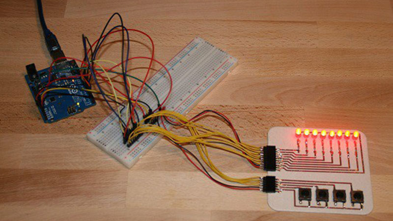
[LudwigLabs] is creating PCBs using copper foil and a cutting plotter (vinyl cutter). In this approach, it’s an additive process where instead of removing copper from a copper-clad board, the traces are cut out of copper foil and transferred to a solid backing surface (cardboard, fiberglass, etc.).
 While similar to the use of copper tape laid out by hand, as covered by us last year, the big advantage of using a cutting plotter is that it allows one to create much more complicated traces similar to those you would expect to see on a factory-made PCB. Since cutting plotters translate a 2D design into very precise movements of the cutting blade, this allows for sharp angles and significantly thinner traces, allows designs from EDA software like KiCad or Altium to be quickly translated to physical boards.
Enterprising hackers might consider the possibility of using this approach to make two-sided, and even multi-layered boards. The copper is produced separately from the substrate which opens up the potential for using uncommon materials like glass or paper to host the circuits. The main limitations are the transferring of (very delicate) copper structures and creating vias without damaging the traces.
As a comparison with traditional PCB fab processes, the photo exposure and etching (or laser exposure and etching) process requires the creation of masks, UV exposing a board, etching, cleaning and so on. The simplicity of copper foil traces has led to many experimenting with this approach. Would you want to use this additive process, or are there refinements or alterations you would make?


It would be interesting to see a hybrid approach to make a 4 layer board, use photmask/etch to create a double sided board with the thinner traces (for comms?) And then use this technique to add two more for power and ground, etc. Although unless you have space constraints it probably won’t be worth the trouble…
I’ve actually been experimenting with something like this. I haven’t needed to do 4 layers, but I did do 2 “bottom” layers with overlapping traces, using a non-conductive vinyl layer in between, in the areas where the traces overlap. I’m not sure what the voltage breakdown would be for such a thin insulating layer, but it should be fine for 3-5V stuff at least. And as a bonus, since the copper tape is also conductive on the glue side, you can make “vias” to connect the two layers easily, just by having a small pad in the same location, with no intermediate vinyl layer. Although, in practice, sometimes it doesn’t seem to make a great connection, so I might add a bit of solder to make sure the 2 layers are connected.
I’ve actually been experimenting with something like this. I haven’t needed to do 4 layers, but I did do 2 “bottom” layers with overlapping traces, using a non-conductive vinyl layer in between, in the areas where the traces overlap. I’m not sure what the voltage breakdown would be for such a thin insulating layer, but it should be fine for 3-5V stuff at least. And as a bonus, since the copper tape is also conductive on the glue side, you can make “vias” to connect the two layers easily, just by having a small pad in the same location, with no intermediate vinyl layer. Although, in practice, sometimes it doesn’t seem to make a great connection, so I might add a bit of solder to make sure the 2 layers are connected.
Also looks like an easy way to achieve 3D integration of circuits for prototyping – assuming that there’s a suitable heat resistant tape under the copper layer it wins out over fancy 4-5 axis lithography and exotic wet chemical processes.
I’ve used this technique to add traces to the bottom of a PLA print. with some through-hole components mounted on the top of the print. (just a flat pcb though, no “3d” traces”). I was able to hand-solder to the pads on the bottom, with no heat resistant tape. I just had to be quick about it to make sure it didn’t heat the PLA up.
Two sided boards could be done by running the cut tape around two edges. The resulting unconnected line on the back of the board could the be bridged bei parts in a suitable format (SOP etc.).
Depending on the insulating properties of the glue, you could also make a third (ground) plane by using a conductive base material.
Also this would be good for adding 3D PCBs to 3D printed parts…
You could also apply the cut PCB during the printing process…
That’s a clever idea! I wonder if they could stack up a board and then try to make vias with a CNC machine or drill press. At least you would have a few more layers to go through. You could also try to sandwich the board in between something to give it some rigidity as well
Coincidentally I saw this guy making solder paste stencils with a vinyl cutter as well.
https://www.youtube.com/watch?v=FrxlQ2l_AHM
When all you got is a hammer …
Not sure what you’re trying to say here. Usually a comment like that implies that you’re using a different tool to do something than normally used, and/or that the tool is misused.
In this case, what would the right tool for a home brewer be?
I think it’s pretty good what he did.
I had this idea some time ago to create flexible PCBs. Just use kapton tape as the base layer, which could also be cut to be user as some kind of solder mask.
Had this idea some time ago to create flexible PCBs. Just use kapton tape as the base layer. One could alo use a cutting plotter and kapton tape to create a solder stop mask.
Excellent. Another excuse to justify getting a cutter.
Anybody have any recommendations for a low price cutter tough enough for this task, but that doesn’t require a cloud service to operate?
All the ones I see are either semipro-grade kilobuck units, or the cheap consumer ones that both look flimsy and usually require cloud connectivity.
I love my silhouette cameo. It doesn’t require a cloud service. It also has an OSS option since someone created a plugin for inkscape.
I too love my Silhouette Cameo for the same reasons.
As for the things you can do with a CNC vinyl cutter, here’s my own project: as I don’t have a paper tape punch for my PDP-11’s (only a reader) I wrote a small utility to actually cut ASCII teletype paper tape using the Cameo:
https://github.com/1944GPW/ptap2dxf
The input is a bin, ptap or any other sort of file. The output is one or more DXF’s that the stencil cutter imports. It really works, and I can read the tapes on my paper tape reader. Long programs are spread over multiple 12″x12″ sticky mat cuts.
See the instruction pdf for examples, and it will make 5-level Baudot RTTY tapes too, as well as pre-war Creed Morse tapes and text banners.
I also use the cutter to make engine and carburetor gaskets for vintage vehicles. My wife uses it for craft!
Getting back to this copper foil cutting idea – it’s great, and I’m going to try it myself. Thanks for the article!
I got a graphtech craft robo on ebay for 28 bucks shipped (with one shitty blade and no 10$ power supply)
it was later rebranded the silhouette cameo SD little bastard is tough, no cloud required and works with the latest (limited but free) software
it gets used either by me or the wife every week and I have shoved 2mm thick cork though it… not that well mind you but it didnt even bog down trying it
the full feature software is like 35 bucks or something
Thanks for the input guys. I’m looking more closely at the Cameo 3 now – I was put off by the software options before, but nice to hear there’s other solutions. LOLs on the TTY tape though — I got rid of my last Model 33 in 1980. I threw my Model 15 off a cliff before that.
I’m not familiar with the cameo 3, or what they go for, but you might check out the “MH” series cutters from uscutter. It looks like they start at $219. I have one of the larger ones and it works fine for this. It accepts hpgl commands over serial (both actual serial, or serial over usb), so you’re not bound to any particular piece of software when using it. I did all my trace layout in inkscape, which has a handy “export to hpgl” functionality.
It seems “US” Cutter takes their name sincerely. From their web page, it’s clear they don’t feel it’s worth selling outside their country’s borders. Their prerogative. Frak ’em. I’ll throw my money somewhere else.
hah, fair enough
The big question for me is whether there’s a thin substrate you could stick the copper to before cutting that would resist being cut itself to provide a sturdy backing to prevent bends or kinks in thin traces or pads during transfer.i have not had a lot of luck with consistent features below 20 mils with any home board process which makes small surface mount parts iffy and I feel this would have the same issue without a very stretch and kink resistent backing that stayed intact while the copper was cut.
These desktop cutters usually come with, and sell in packs, adhesive “cutting mats” for precisely this purpose. They are available in a variety of sizes and degrees of adhesion.
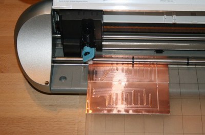
This is exactly what vinyl cutters do. The medium that you’re cutting will have a backing paper on it, and the blade on the vinyl cutter is set so that it just barely pokes out of the blade holder. So that when you’re cutting, it cuts just the medium being cut (e.g. vinyl, or in this case copper foil), without cutting through the paper backing. The paper backing provides enough support to mostly keep the copper in place as you’re cutting it, although there is still a bit of a tendency for the pads to lift up during the cutting process. I was able to mostly mitigate this by using a 60 degree blade, and going as slow as my cutter allows.
The most time consuming process is removing all the extra material (i.e. “weeding”) afterward. It’s easy to accidentally lift up the traces, so you have to be very slow and methodical about removing the unwanted areas of copper.
Is there a copper foil 12″ wide roll available for large vinyl cutters?
Here is also another version, without transfer foil:
English: https://projekte.simonbrem.de/plotter-platinen/en/plotter-platinen_en.html
German: http://projekte.simonbrem.de/plotter-platinen/de/plotter-platinen.html